
Thinner silicon wafers promise more wafers per ingot and less material per device or solar cell. The apparent lever is simple: reduce wafer thickness and use a finer wire. In production, the lever is connected to wire stiffness, breakage, saw marks, wafer bow, handling and downstream yield. A few micrometers saved in geometric kerf can be lost through extra grinding, broken wafers or conservative machine speed.
A 2026 review of ultra-fine diamond wire slicing identifies wire breakage, saw marks, wafer warp and wire wear among the main challenges as wire diameters move below 35 micrometers in thin-wafer production. Much of the volume pressure comes from photovoltaics, but the process logic also matters for semiconductor substrates and research wafers: the target is not the thinnest as-cut piece. It is the highest number of accepted wafers per ingot at stable cost.
This guide explains how to qualify ultra-fine diamond wire saw slicing without treating wire diameter as the only design variable.

Why thin-wafer economics are nonlinear
Ingot utilization improves when each wafer consumes less thickness and less kerf. A first estimate divides usable ingot length by wafer thickness plus kerf. Real output is lower because the process also needs end allowances, thickness margin, finishing stock and yield losses.
A practical material-yield model includes:
- as-cut wafer thickness and wafer-to-wafer variation;
- measured kerf, including abrasive envelope and wire motion;
- stock removed in cleaning, texturing, grinding, lapping or polishing;
- wafers lost to breakage, chips, cracks, TTV, bow or warp;
- wire breaks and partial ingot recovery;
- handling and downstream yield by wafer thickness.
The optimum can sit above the minimum achievable thickness. Procurement should compare cost per accepted wafer and accepted surface area, not nominal wafers per ingot.
What changes when diamond wire becomes ultra-fine
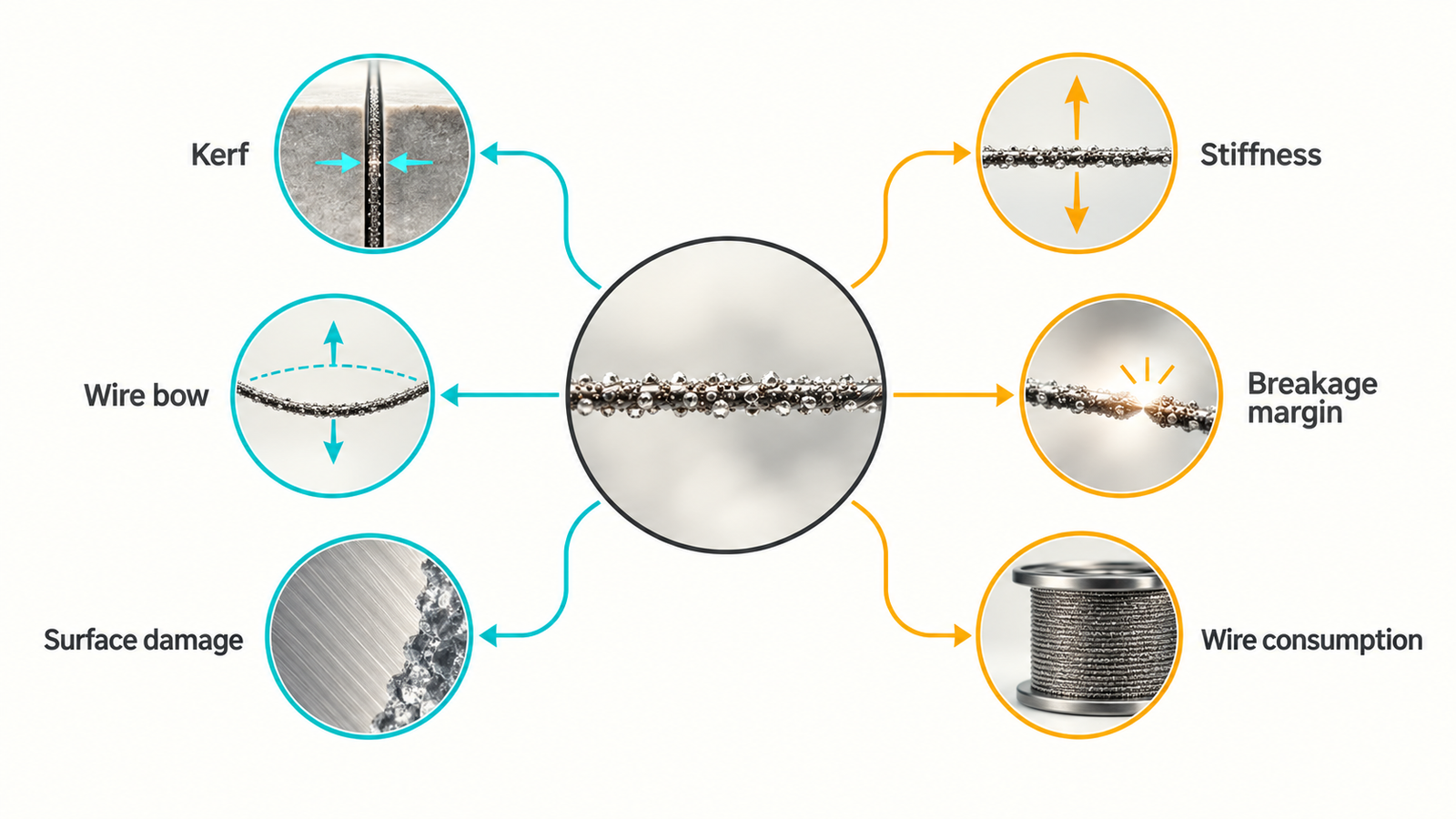
Reducing core diameter lowers cross-sectional area and bending stiffness. The wire has less tensile margin and deflects more under the same lateral load. Bond volume and the number of well-supported abrasive grains may also change. Manufacturing variation that was harmless on a larger wire becomes more important.
Four trade-offs dominate:
- Kerf versus stiffness. A finer wire can reduce geometric loss but is more sensitive to bow, vibration and groove condition.
- Grain size versus removal. Fine abrasive can improve surface texture, while insufficient chip space raises loading and heat.
- Tension versus fatigue. Tension limits deflection but increases stress and demand on guides and the core.
- Wire consumption versus quality. Using less new wire can reduce consumable cost while increasing wear-related waviness and breakage.
Recent research on wire deflection reports that overly aggressive reductions in wire use can worsen waviness and breakage, while moderate consumption improves reliability. The useful conclusion is to optimize material and wire together.
Control wire bow before chasing speed
Feed force bends the wire web. As contact length increases, removal resistance and bow can rise. If the wire lags behind the programmed feed, its later recovery leaves thickness error or saw marks. Fine wire increases the sensitivity.
Monitor drive current, feed load, tension response, wire speed and cut position. Where possible, use a calibrated direct or soft-sensor estimate of bow. Adjust feed with contact length instead of applying one value through the entire ingot. Protect entry and exit, where support and engagement change rapidly.
Higher wire speed can increase abrasive engagements, but it may also raise vibration, heat and wear. Higher tension can reduce bow, but it narrows the breakage margin. The stable window is a combination of wire, speed, feed, tension, coolant and guide condition.
Guide grooves become more critical
Ultra-fine wire needs compatible groove pitch, profile and surface condition. A groove designed around a larger wire may not seat or guide a smaller one correctly. Wear can add torsion or lateral movement. Inspect groove geometry, runout, wire seating and lane-to-lane condition before attributing marks to the material.
Web alignment should be checked relative to the ingot datum. For thin wafers, a small pitch or parallelism error consumes a larger fraction of the product thickness. Keep wafer identity by lane so damaged grooves and coolant zones can be found.
Coolant and particle control at narrow kerf
A narrower kerf leaves less space for coolant and debris transport. Silicon chips and worn abrasive can recirculate, increasing scratches and local force. Verify flow at the web rather than pump capacity alone. Track filter differential pressure, fluid temperature, concentration and solids.
Nozzle uniformity matters across a wide web. Edge lanes can run hotter or receive weaker flushing. Excessive jets can disturb the finest wires, so balance flow and mechanical stability. A coolant and debris-removal plan should be part of the wire-diameter trial.
Thin wafers shift risk into handling
A slicing process can improve while total yield falls because thinner wafers break during separation, cleaning or transfer. Include unloading, adhesive release, washing, drying, cassette loading and robotic pickup in the qualification.
Measure wafer shape after a standardized relaxation and support condition. TTV, bow and warp are different outputs. Residual stress and damage can cause wafers to distort when released from a beam or adhesive. Track the direction of curvature relative to wire travel and ingot orientation.
Downstream teams should test the same thickness distribution produced by the saw, not specially selected flat wafers. A process is ready when ordinary wafers survive the normal route.
A stepwise ultra-fine wire qualification
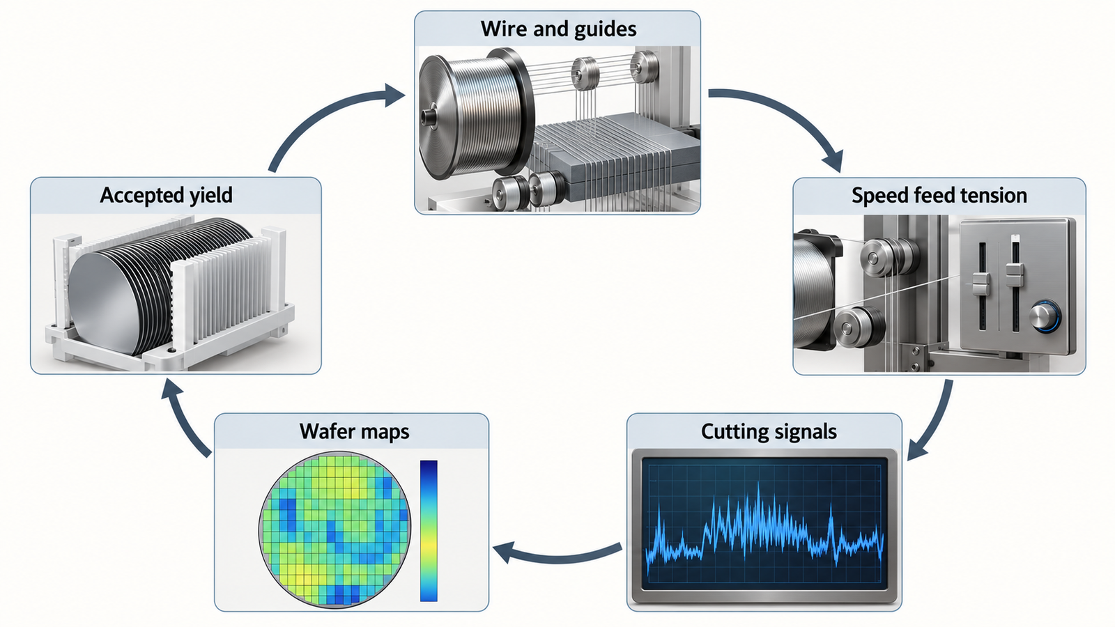
- Establish the current baseline. Record kerf, wire use, cycle time, breakage, geometry, surface, finishing and accepted yield.
- Change one wire family. Document core diameter, abrasive, bond, supplier lot and compatible guide setup.
- Confirm machine readiness. Check guides, alignment, tension calibration, coolant and data logging.
- Develop a safe process window. Screen feed, speed and tension around conservative conditions using representative contact length.
- Run full ingots. Coupons cannot reveal all web, thermal and handling effects.
- Map lane and sequence. Measure thickness, TTV, bow, warp, surface marks and chips across the web.
- Test wire-life stages. Include conditioned and later-life wire rather than only fresh wire.
- Complete downstream processing. Measure breakage and stock removal through the accepted wafer.
- Calculate economics. Compare ingot yield, wire cost, uptime, labor and accepted wafers.
Multi-wire and endless system roles
A diamond multi-wire saw for semiconductor and photovoltaic wafer cutting is the main architecture for high-volume parallel silicon slicing. It must demonstrate web-wide consistency, controlled wire consumption and reliable handling.
An endless diamond wire saw serves a different role. It can prepare research wafers, special silicon components, defect coupons and small batches. It also provides a flexible platform for comparing support, orientation and wire behavior before a large multi-wire trial.
Do not extrapolate throughput directly between architectures. Compare each system against its intended volume, geometry and learning objective.
Metrics for an equipment or wire decision
| Metric | Why it matters |
|---|---|
| Measured kerf distribution | Shows actual material loss, not catalog wire diameter |
| Accepted wafers per ingot | Combines thickness, kerf and yield |
| Wire consumption per accepted wafer | Connects consumable policy to quality |
| Breaks and recovery time | Captures downtime and at-risk ingot value |
| TTV, bow, warp and marks | Protects downstream handling and finishing |
| Finishing stock | Reveals hidden slicing damage |
| Downstream survival | Confirms the thin wafer is manufacturable |
How ewirexon supports silicon wafer slicing
Ewirexon supplies diamond multi-wire saw and endless diamond wire saw solutions for silicon wafer slicing, SiC, sapphire and other brittle materials. A thin-wafer project should begin with ingot size, silicon type, target thickness, kerf objective, surface and shape limits, finishing route, annual capacity and handling constraints.
A sample and pilot plan can then compare wire systems using raw lane-level data and cost per accepted wafer. Where ultra-fine wire requires guide, tension or fluid changes, those dependencies should be included in the equipment scope and acceptance test.
Conclusion
Ultra-fine diamond wire creates a real opportunity to reduce silicon kerf, but it also reduces mechanical margin. Wire bow, groove condition, coolant delivery, wear and handling become more important as both wire and wafer become thinner.
Qualify the complete manufacturing path and calculate accepted wafers per ingot. The winning process may not use the smallest wire or fastest feed. It will use the narrowest stable process window that production can maintain through normal wire life, operators and downstream handling.
Frequently asked questions
What is ultra-fine diamond wire for silicon slicing?
Recent literature commonly discusses wire below about 35 micrometers in thin-wafer production. The exact practical range depends on wire construction, machine and product requirements.
Does thinner diamond wire always reduce kerf loss?
It reduces geometric potential, but bow, vibration, breakage and finishing damage can erase the gain. Measure total material loss through final acceptance.
Why do thin silicon wafers warp?
Thickness variation, residual stress, asymmetric damage, mounting and release can all contribute. Measure bow and warp under a standardized method and preserve cutting direction.
How can wire breakage be reduced?
Use compatible guides, calibrated tension, smooth speed changes, controlled feed, effective cooling and a replacement limit based on wire exposure and condition.
What is the best KPI for thin-wafer slicing?
Accepted wafers per ingot or cost per accepted wafer is more useful than kerf or cycle time alone because it includes geometry, breakage, finishing and handling yield.
Technical references
- Progress and critical challenges in slicing thin semiconductor wafers with ultra-fine diamond wire, 2026.
- Wire deflection, waviness and wire-consumption trade-offs, 2026.
- Review of silicon wafering technology and material utilization, 2025.
Editorial note: Wire limits and wafer thickness capability depend on the complete equipment and downstream process. The figures are AI-generated engineering illustrations, not customer production data.