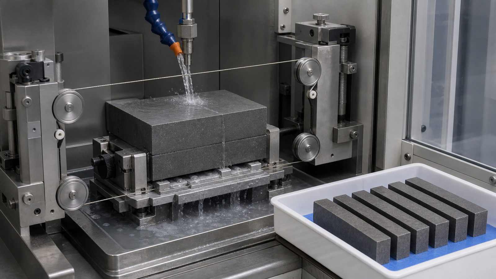








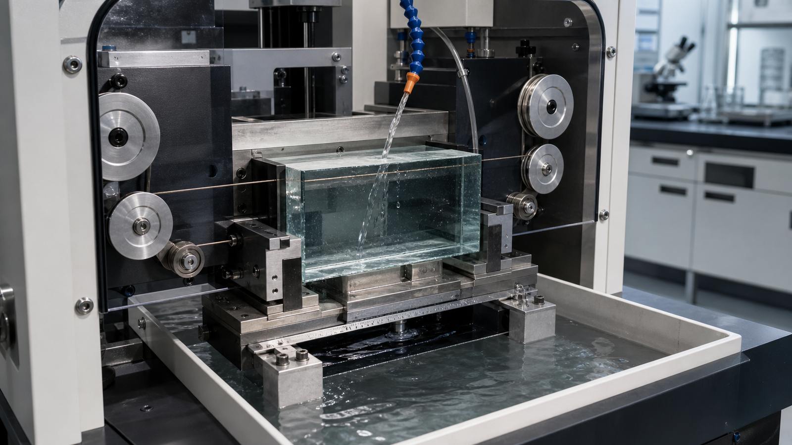
Diamond Wire Saw for Glass Core Substrate R&D: Where It Fits and Where It Does Not
Learn where diamond wire sawing fits in glass core substrate R&D, how to control edge damage, and when laser or blade singulation is the better choice.
Diamond Wire Cutting Systems for Package Substrate Slicing & Precision Component Cutting
Chip carrier and package material precision cutting systems can make the difference between yield and scrap in high-volume semiconductor packaging. They provide a reliable processing solution by cutting brittle, multi-layer packaging substrates and lead frames with ultra-high accuracy. Especially for packaging manufacturers, many factors have to be kept in mind in order to be able to guarantee the dimensional accuracy and structural integrity of the components.
In order to process multi-layer packaging materials with complex structures and high hardness, a stable cutting process must be achieved with minimal kerf loss and sub-surface damage. To ensure that the increasing precision requirements of advanced packaging do not lead to component defects or yield loss, the performance of the cutting systems used must be guaranteed at all times. In order to be able to guarantee this performance, diamond wire cutting systems must be tested in accordance with semiconductor industry standards at accredited testing laboratories.
Industry-standard certified cutting systems are subject to defined guidelines with regard to process modifications. ewirexon uses a special production and process optimization process to help you ensure that the high qualitative requirements of advanced packaging are met.
ewirexon diamond wire cutting systems for package material processing are characterized by an optimum price/performance ratio and are particularly suitable for precision cutting of chip carriers, lead frames and multi-layer packaging substrates. The systems generate ultra-high cutting accuracy with minimal kerf loss in limited production space. With rigid machine frames that can meet the strict precision requirements of advanced packaging, ewirexon offers an efficient and reliable option for fabs that handle both R&D prototyping and high-volume production at the same time. Thanks to a wide range of performance and customized process parameters, manufacturers of semiconductor packaging can reduce their component diversity with ewirexon’s Package Material Cutting solution.
| NO. | Parameter | Specification |
| 1 | Model | TCQF400LNC-FM-HL |
| 2 | Cutting Principle | Endless diamond wire / Physical cutting |
| 3 | Cutting Functions | Slicing / Angle & Profile Cutting |
| 4 | Maximum Workpiece Size(mm) | Φ600mm, Height 500mm |
| 5 | Worktable Size(mm) | Ø380 转台 |
| 6 | Cutting Planarity Accuracy(mm) | 0.08 |
| 7 | Surface Roughness(μm) | Ra 0.8μm |
| 8 | Wire Specification(mm) | Ø0.65–1.0/2580 |
| 9 | Tension System | Constant Wire Tension Control |
| 10 | Guide Wheel Quantity | 4 wheels |
| 11 | Drive Motor | Servo motor |
| 12 | Wire Speed (m/s) | 51Max(Adjustable) |
| 13 | Total Power(kW) | 2.8 |
| 14 | Voltage | 220v 50Hz |
| 15 | Control System | Custom-developed Tongcheng T32 system |
| 16 | Footprint (L×W×H)(mm) | 1350×1066×1968 |
| 17 | Gross Weight kg | 720 |
In the demanding semiconductor packaging industry, certified high-precision cutting solutions are indispensable. This case study looks at the complex challenge of developing a high-yield diamond wire cutting system that has to process ultra-thin, multi-layer packaging materials reliably with minimal kerf loss. How was our customer able to not only meet the strict precision requirements of advanced packaging, but even exceed them? What role did the strategic partnership with ewirexon play in this challenging project?
Want to know more project cases? Feel free to write us!

Learn where diamond wire sawing fits in glass core substrate R&D, how to control edge damage, and when laser or blade singulation is the better choice.

Learn how to control waviness, chipping, wire wear and material loss in NdFeB magnet cutting with a diamond wire saw and a measurable trial plan.
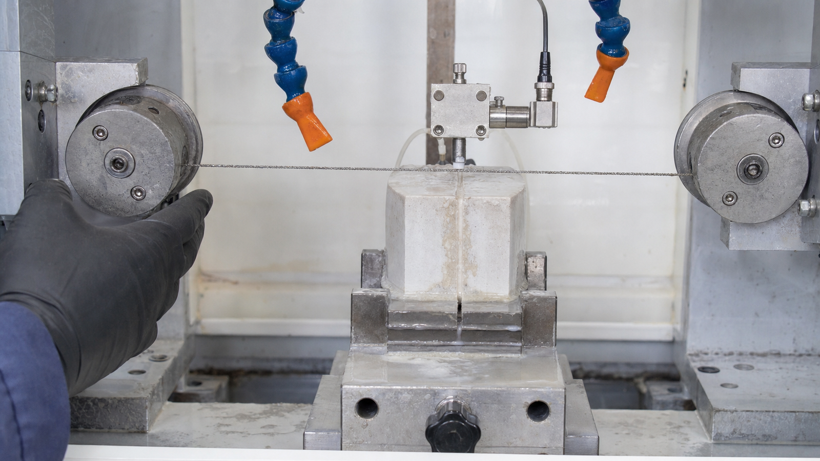
Diagnose diamond wire saw breakage using wire-path, tension, load, coolant, wear, and fixture evidence instead of trial-and-error parameter changes.
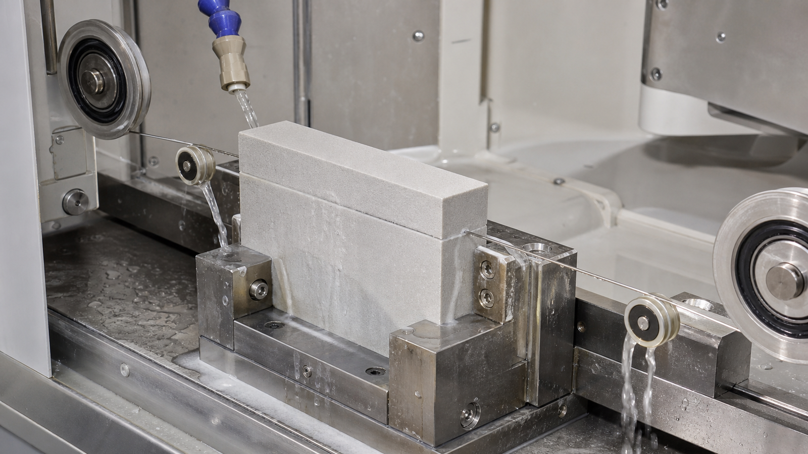
Learn how to qualify a diamond wire saw process for AlN substrate cutting, control chipping and subsurface damage, and select lab or production equipment.
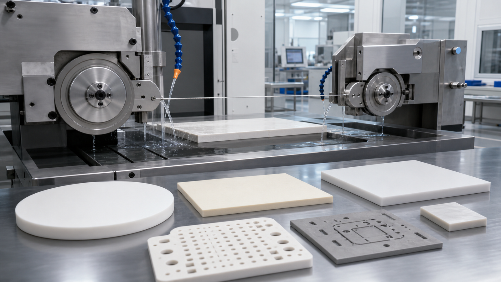
Learn how diamond wire saw technology improves advanced ceramic cutting for semiconductor packaging, power electronics and precision components.
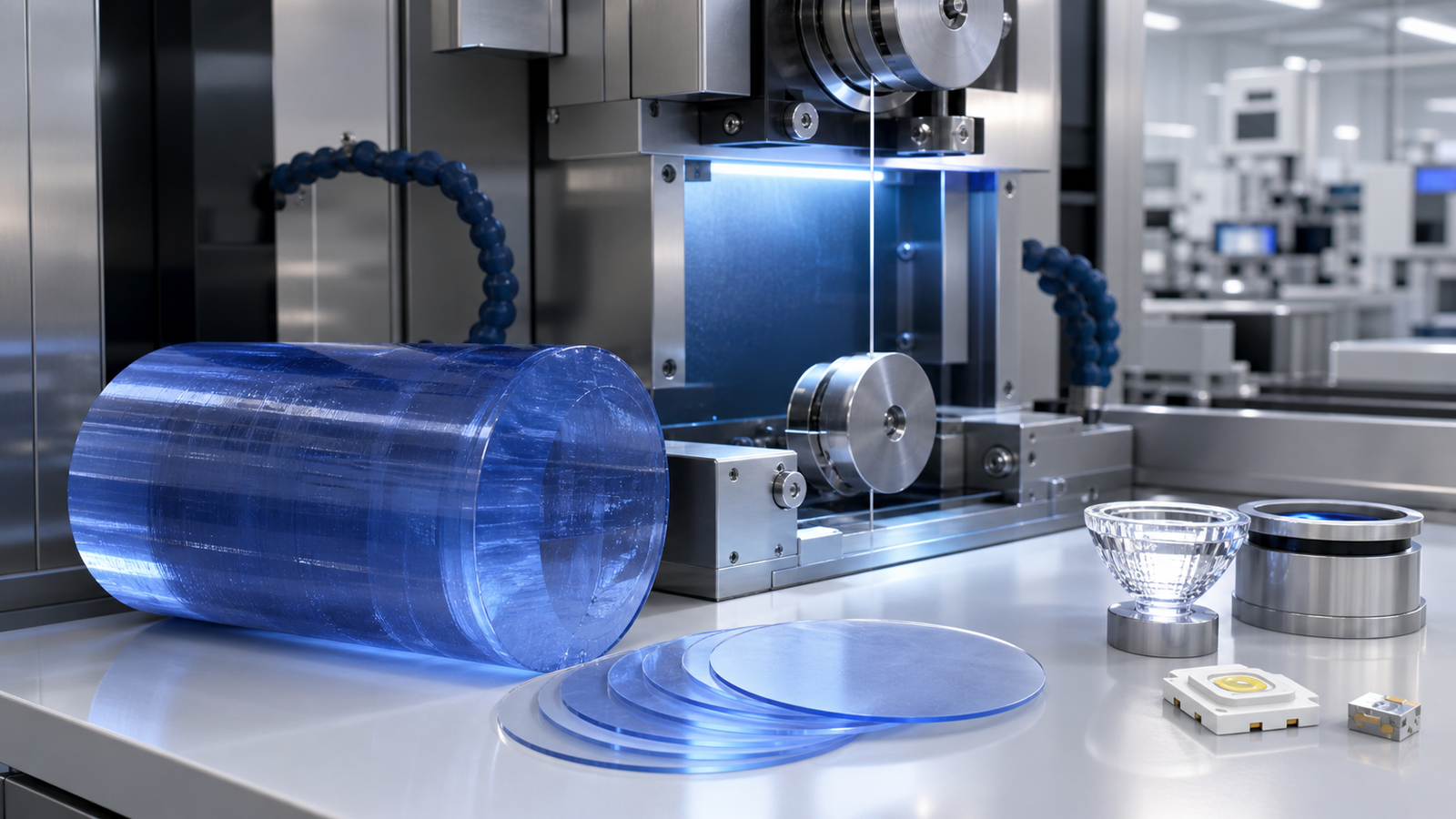
Explore how diamond wire saw technology improves sapphire substrate cutting for LED, RF, optical and semiconductor applications.

ewirexon.com
Typically replies within minutes
Hi, there, is there anything do for you ?
WhatsApp Us
🟢Online | Privacy policy
WhatsApp us