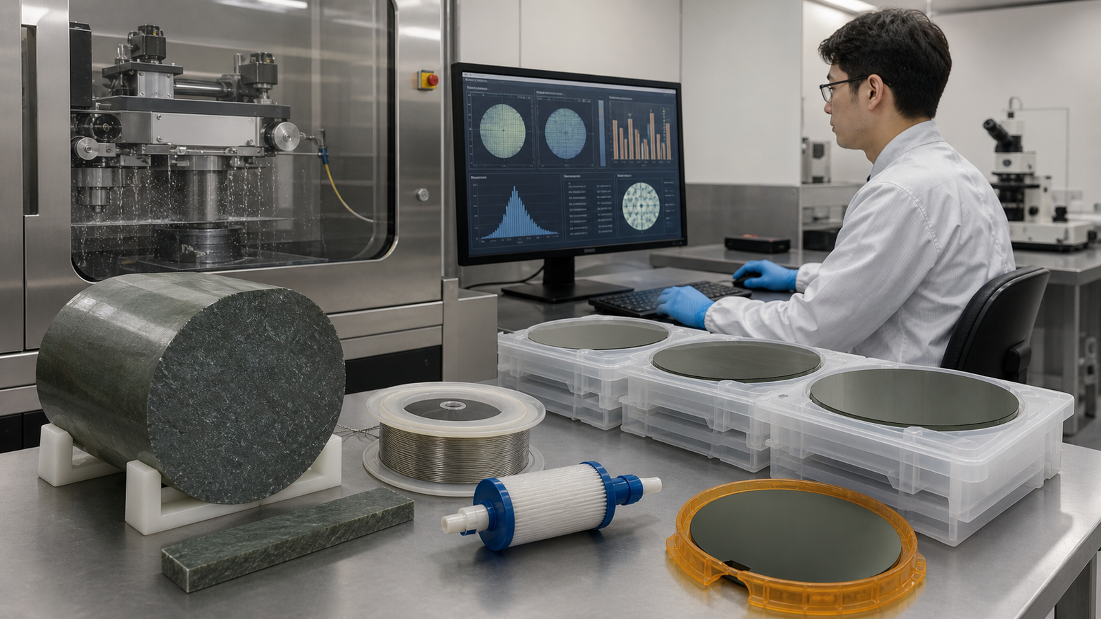








Diamond Wire Saw for Glass Core Substrate R&D: Where It Fits and Where It Does Not
Learn where diamond wire sawing fits in glass core substrate R&D, how to control edge damage, and when laser or blade singulation is the better choice.
Diamond Wire Cutting Systems for Electronic Ceramic Substrate Manufacturing & Dicing
Electronic ceramic substrates are used in a wide variety of semiconductor and electronic manufacturing processes. Without sufficient precision cutting, the dimensional errors and material damage generated during substrate processing can lead to reduced device performance, increased yield loss and consequential failure of the end product. To ensure optimum functionality of multi-layer ceramic components, power modules and electronic packages at all times and to minimize production downtime, reliable, high-precision substrate processing must be ensured.
In addition to ultra-tight dimensional accuracy to meet the packaging requirements, the diamond wire cutting systems used should meet other requirements. Among other things, semiconductor industry quality standards must be complied with, which means that the cutting systems must have very low kerf loss and minimal sub-surface damage. Furthermore, there are high requirements for process stability, for example when used in high-volume production lines, so the systems must be designed so that there is consistent, repeatable cutting performance. In addition, a compact footprint is of great importance when integrated into automated substrate manufacturing lines with limited factory space.
With the Electronic Ceramic Substrate Processing Line, ewirexon supplies some of the world’s most high-precision and at the same time most cost-effective diamond wire cutting systems for electronic ceramic substrate manufacturing. Specially developed for slicing alumina, aluminum nitride (AlN) and multi-layer ceramic substrates, the cutting systems deliver ultra-tight dimensional accuracy with a very compact and robust design. Thus, the systems enable a space-saving production line design even at high throughput and variable processing parameters. Thanks to the low kerf loss of the cutting systems, material yield can be maximized depending on the substrate type.
| NO. | Parameter | Specification |
| 1 | Model | TCQF400LNC-FM-HL |
| 2 | Cutting Principle | Endless diamond wire / Physical cutting |
| 3 | Cutting Functions | Slicing / Angle & Profile Cutting |
| 4 | Maximum Workpiece Size(mm) | Φ600mm, Height 500mm |
| 5 | Worktable Size(mm) | Ø380 转台 |
| 6 | Cutting Planarity Accuracy(mm) | 0.08 |
| 7 | Surface Roughness(μm) | Ra 0.8μm |
| 8 | Wire Specification(mm) | Ø0.65–1.0/2580 |
| 9 | Tension System | Constant Wire Tension Control |
| 10 | Guide Wheel Quantity | 4 wheels |
| 11 | Drive Motor | Servo motor |
| 12 | Wire Speed (m/s) | 51Max(Adjustable) |
| 13 | Total Power(kW) | 2.8 |
| 14 | Voltage | 220v 50Hz |
| 15 | Control System | Custom-developed Tongcheng T32 system |
| 16 | Footprint (L×W×H)(mm) | 1350×1066×1968 |
| 17 | Gross Weight kg | 720 |

Learn where diamond wire sawing fits in glass core substrate R&D, how to control edge damage, and when laser or blade singulation is the better choice.

Learn how to control waviness, chipping, wire wear and material loss in NdFeB magnet cutting with a diamond wire saw and a measurable trial plan.

Diagnose diamond wire saw breakage using wire-path, tension, load, coolant, wear, and fixture evidence instead of trial-and-error parameter changes.

Learn how to qualify a diamond wire saw process for AlN substrate cutting, control chipping and subsurface damage, and select lab or production equipment.

Learn how diamond wire saw technology improves advanced ceramic cutting for semiconductor packaging, power electronics and precision components.

Explore how diamond wire saw technology improves sapphire substrate cutting for LED, RF, optical and semiconductor applications.
ewirexon.com
Typically replies within minutes
Hi, there, is there anything do for you ?
WhatsApp Us
🟢Online | Privacy policy
WhatsApp us