






Резка электронных керамических подложек


Diamond Wire Cutting Systems for Electronic Ceramic Substrate Manufacturing & Dicing

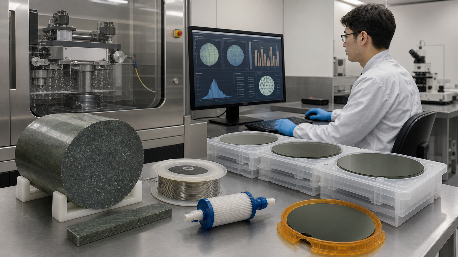
Electronic ceramic substrates are used in a wide variety of semiconductor and electronic manufacturing processes. Without sufficient precision cutting, the dimensional errors and material damage generated during substrate processing can lead to reduced device performance, increased yield loss and consequential failure of the end product. To ensure optimum functionality of multi-layer ceramic components, power modules and electronic packages at all times and to minimize production downtime, reliable, high-precision substrate processing must be ensured.

In addition to ultra-tight dimensional accuracy to meet the packaging requirements, the diamond wire cutting systems used should meet other requirements. Among other things, semiconductor industry quality standards must be complied with, which means that the cutting systems must have very low kerf loss and minimal sub-surface damage. Furthermore, there are high requirements for process stability, for example when used in high-volume production lines, so the systems must be designed so that there is consistent, repeatable cutting performance. In addition, a compact footprint is of great importance when integrated into automated substrate manufacturing lines with limited factory space.

ewirexon Electronic Ceramic Substrate Processing

Electronic Ceramic Substrate Cutting Systems

With the Electronic Ceramic Substrate Processing Line, ewirexon supplies some of the world’s most high-precision and at the same time most cost-effective diamond wire cutting systems for electronic ceramic substrate manufacturing. Specially developed for slicing alumina, aluminum nitride (AlN) and multi-layer ceramic substrates, the cutting systems deliver ultra-tight dimensional accuracy with a very compact and robust design. Thus, the systems enable a space-saving production line design even at high throughput and variable processing parameters. Thanks to the low kerf loss of the cutting systems, material yield can be maximized depending on the substrate type.

  • Easier maintenance and assembly
  • thanks to modular, user-friendly system design.
  • Favors space-saving production line design
  • as the particularly compact cutting systems allow for a streamlined layout of the overall manufacturing cell.
  • Competitive advantage due to cost savings
  • as the highly efficient cutting process allows the use of standard production lines without costly custom modifications, maximizing material yield and reducing waste.
  • Avoidance of downtimes / low wear
  • The robust design of the cutting system allows it to be used even at high speeds and in continuous 24/7 production environments.
  • Short delivery times, low transport costs.
  • Electronic ceramic substrate slicing & dicing
  • Processing of AlN, alumina and multi-layer ceramic substrates
  • High-precision cutting for power electronic packages
  • Substrate manufacturing for semiconductor components
  • Ceramic component processing for electronic devices
НЕТ.ПараметрТехнические характеристики
1МодельTCQF400LNC-FM-HL
2Принцип резкиБесконечная алмазная леска / Механическая резка
3Функции резкиНарезка / Резка под углом и по профилю
4Максимальный размер заготовки (мм)Φ600 мм, высота 500 мм
5Размер рабочего стола (мм)Ø380 转台
6Точность плоскостности реза (мм)0.08
7Шероховатость поверхности (мкм)Ra 0,8 мкм
8Характеристики проволоки (мм)Ø0,65–1,0/2580
9Система натяженияКонтроль постоянного натяжения проволоки
10Количество направляющих колес4 колеса
11Приводной двигательСервомотор
12Скорость движения проволоки (м/с)51Max (регулируемый)
13Общая мощность (кВт)2.8
14Напряжение220 В, 50 Гц
15Система управленияСпециально разработанная система Tongcheng T32
16Габаритные размеры (Д × Ш × В) (мм)1350×1066×1968
17Брутто-вес, кг720
9

Case Study: Electronic Ceramic Substrate Processing

A ceramic products manufacturer partnered with ewirexon to upgrade their cutting process, achieving higher yield, lower material waste, and consistent precision in production.
Хотите узнать больше о наших проектах? Не стесняйтесь, пишите нам!

Напишите нам!

Загрузите свои 2D-чертежи и как минимум один 3D-файл CAD, чтобы получить расчет стоимости быстрее и точнее. Если у вас несколько файлов, скомпрессируйте их в архив формата .zip или .rar. Предпочитаете электронную почту? Отправьте запрос на расчет стоимости по адресу info@xxx.com.

Новости и обновления