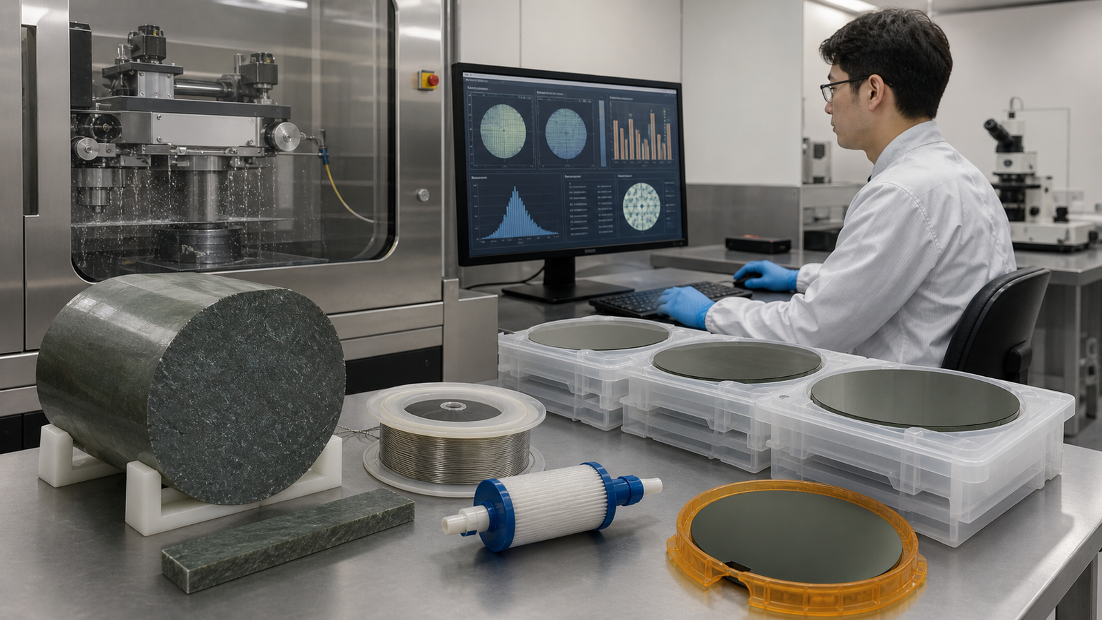









Нарезка основного материала печатной платы


High-Precision Wire Saw Systems for Electronic Substrate Processing

Rigid, flexible, and rigid-flex circuit substrates form the backbone of electronic devices, from consumer gadgets to industrial control systems. Precision slicing of these substrates is essential to maintain circuit integrity, flatness, and electrical performance. Diamond wire cutting provides a damage-free alternative to traditional methods, preserving substrate properties and eliminating delamination.

Our specialized systems deliver precise, clean slicing for FR-4, ceramic, polyimide, and copper-clad laminates, ensuring consistent thickness and flatness across large-format panels. The closed-loop tension control and real-time monitoring prevent micro-cracks and fiber damage, critical for high-density, fine-pitch circuit boards.

Suitable for both R&D prototyping and mass production, our solutions support high-throughput processing for multi-layer PCBs and advanced circuit substrates. The intelligent CNC control allows for precise parameter adjustment, ensuring compatibility with the latest PCB technologies and flexible circuit manufacturing processes.

Precision Slicing Systems for PCB & Circuit Substrates


Our diamond wire cutting solutions are tailored for high-precision slicing of rigid, flexible, and rigid-flex PCB base materials, ceramic substrates, and semiconductor packaging substrates. The systems feature closed-loop tension control and real-time monitoring, ensuring consistent thickness, flatness, and damage-free cutting for high-density, fine-pitch circuit boards. This eliminates delamination and micro-cracks, directly improving PCB yield and reliability in mass production.

Нарезка подложки и материала основания печатной платы

Преимущества
  • Damage-Free Processing: Prevents substrate delamination and fiber damage, critical for high-frequency PCB performance.
  • Consistent Thickness Control: Maintains uniform substrate thickness across large panels, ensuring stable circuit etching.
  • High Compatibility: Supports a full range of substrate materials, including FR-4, ceramic, polyimide, and copper-clad laminates.
  • High-Efficiency Mass Production: Multi-wire cutting design reduces processing time per panel, lowering production costs.
  • PCB base material slicing for consumer and automotive electronics
  • Ceramic substrate cutting for semiconductor packaging and power modules
  • Flexible circuit substrate processing for wearable and 5G devices
НЕТ.ПараметрТехнические характеристики
1МодельTCQF400LNC-FM-HL
2Принцип резкиБесконечная алмазная леска / Механическая резка
3Функции резкиНарезка / Резка под углом и по профилю
4Максимальный размер заготовки (мм)Φ600 мм, высота 500 мм
5Размер рабочего стола (мм)Ø380 转台
6Точность плоскостности реза (мм)0.08
7Шероховатость поверхности (мкм)Ra 0,8 мкм
8Характеристики проволоки (мм)Ø0,65–1,0/2580
9Система натяженияКонтроль постоянного натяжения проволоки
10Количество направляющих колес4 колеса
11Приводной двигательСервомотор
12Скорость движения проволоки (м/с)51Max (регулируемый)
13Общая мощность (кВт)2.8
14Напряжение220 В, 50 Гц
15Система управленияСпециально разработанная система Tongcheng T32
16Габаритные размеры (Д × Ш × В) (мм)1350×1066×1968
17Брутто-вес, кг720
0

Read the Case: Improve PCB Base Material Slicing Quality

Professional PCB base material slicing enterprises adopted our solutions to upgrade equipment and workflows, gaining higher yield, lower waste and reliable slicing precision.
Хотите узнать больше о наших технических примерах? Свяжитесь с нами.

Напишите нам!

Загрузите свои 2D-чертежи и как минимум один 3D-файл CAD, чтобы получить расчет стоимости быстрее и точнее. Если у вас несколько файлов, скомпрессируйте их в архив формата .zip или .rar. Предпочитаете электронную почту? Отправьте запрос на расчет стоимости по адресу info@xxx.com.

Новости и обновления