







Прецизионная обработка оптических пластин


Diamond Wire Cutting Systems for Optical Wafer Slicing, LED Substrate Dicing, and Photonic Wafer Processing

In high-volume optoelectronic and semiconductor manufacturing, the precise, low-stress slicing of optical wafers and sapphire substrates is a critical process that directly impacts material yield, production efficiency, and final device performance.

To meet these demands, diamond wire cutting equipment must maintain a stable operating point with exceptional dimensional accuracy and consistent process control, whether deployed in multi-wire saws for high-throughput production or single-wire systems for ultra-precision applications. Similar technical rigor is required for photonic wafer processing and LED substrate dicing, where even tighter thickness tolerances and superior surface flatness are essential for high-performance optoelectronic devices.

Beyond core cutting performance, modern wafer processing equipment must also deliver long-term operational value: minimal material waste and sub-surface damage to reduce raw material costs, high reliability and energy efficiency for cleanroom production environments, and optimized material utilization to offset rising input costs. These factors make diamond wire cutting systems increasingly critical for cost-effective, scalable optoelectronic manufacturing.

Precision Optical Wafer Processing Systems

Precision Optical Wafer Processing Systems

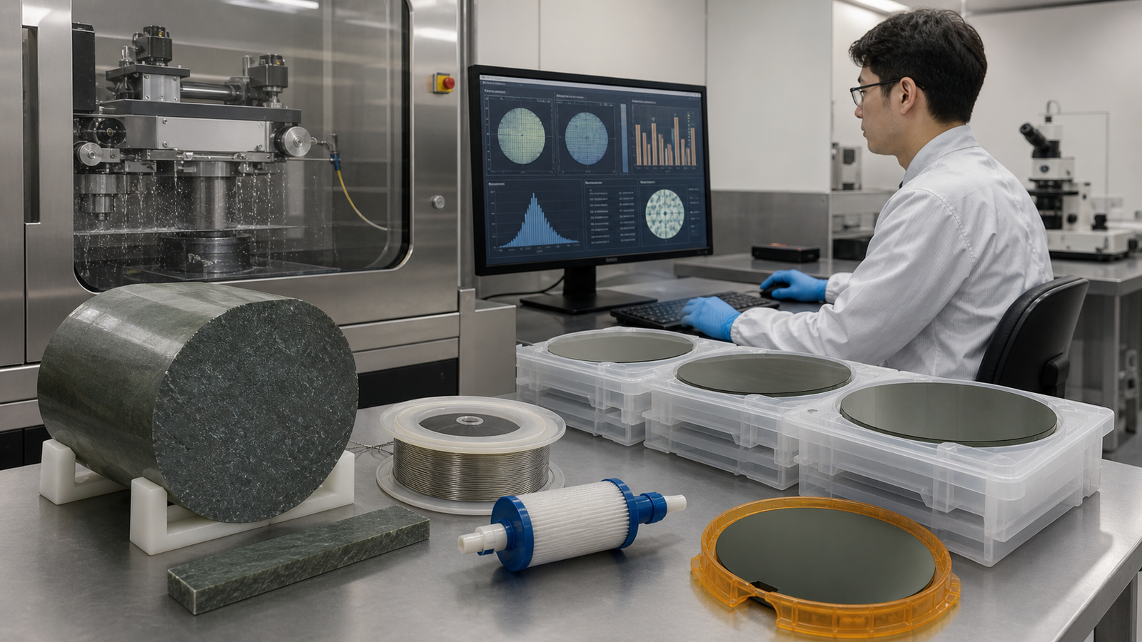
The Precision Optical Wafer Processing systems are specially designed for optical wafer slicing, LED sapphire substrate dicing, and photonic crystal wafer processing. For these applications, ewirexon offers configuration options with high-precision multi-wire saws as well as single-wire cutting units. Both options feature an extremely stable, vibration-damped steel frame design. The multi-wire system achieves very high production efficiency (high volume, ultra-low kerf loss) in a compact footprint, while the single-wire unit delivers superior dimensional accuracy for thin wafers. Both options integrate seamlessly into automated wafer processing lines and can be swapped depending on production requirements, enabling ideal alignment to customer-specific manufacturing workflows with minimal setup changes.

  • Lower service costs
  • robust vibration-damped frame with optimised material thickness extends system lifespan.
  • Easier maintenance and installation
  • lightweight modular design with quick-access wire tension system reduces downtime.
  • Maximum material cost savings
  • ultra-low kerf loss cutting significantly reduces raw material waste in high-value wafer processing.
  • Flexible system design / easy replacement
  • standard wafer chuck dimensions and multi-cut mode support for diverse wafer types.
  • Fast and cost effective delivery
  • Optical wafer slicing / LED substrate dicing
  • Sapphire & quartz wafer processing for optoelectronics
  • Photonic crystal wafer dicing & precision optical component manufacturing
  • Automated high-volume wafer production lines for optics & semiconductors
НЕТ.ПараметрТехнические характеристики
1МодельTCQF600PNC
2Принцип резкиБесконечная алмазная леска / Механическая резка
3Функции резкиFlat Cutting / Rotary Slicing
4Максимальный размер заготовки (мм)200 × 200 × 220 mm (L×W×H)
5Размер рабочего стола (мм)Ø600 转台
6Точность плоскостности реза (мм)0.1
7Шероховатость поверхности (мкм)Ra 0,8 мкм
8Характеристики проволоки (мм)0.65–1.0/3720
9Система натяженияКонтроль постоянного натяжения проволоки
10Количество направляющих колес3 колеса
11Приводной двигательСервомотор
12Скорость движения проволоки (м/с)51Max (регулируемый)
13Общая мощность3.3
14Напряжение380v 50Hz
15Система управленияCustom-developed Tongcheng T30 system
16Габаритные размеры (Д × Ш × В) (мм)1650×1750×2010
17Брутто-вес, кг1250
ewirexon - ewirexon precision diamond wire cutting system

Case Sharing: Optimize Your Optical Wafer Processing Workflow

We collaborated with a precision optical wafer enterprise to refine manufacturing techniques. The project delivered improved yield performance, reduced raw material waste and outstanding precision consistency.
Хотите узнать больше о наших технических примерах? Свяжитесь с нами.

Напишите нам!

Загрузите свои 2D-чертежи и как минимум один 3D-файл CAD, чтобы получить расчет стоимости быстрее и точнее. Если у вас несколько файлов, скомпрессируйте их в архив формата .zip или .rar. Предпочитаете электронную почту? Отправьте запрос на расчет стоимости по адресу info@xxx.com.

Новости и обновления