








ガラスコア基板の研究開発におけるダイヤモンドワイヤーソー:適している用途とそうでない用途
ダイヤモンドワイヤーソーがガラスコア基板の研究開発においてどのような役割を果たすのか、エッジの損傷をどのように抑制するのか、また、レーザーやブレードによる個片化のどちらが適しているのかについて学びましょう。.
Diamond Wire Cutting Systems for Optical Wafer Slicing, LED Substrate Dicing, and Photonic Wafer Processing
In high-volume optoelectronic and semiconductor manufacturing, the precise, low-stress slicing of optical wafers and sapphire substrates is a critical process that directly impacts material yield, production efficiency, and final device performance.
To meet these demands, diamond wire cutting equipment must maintain a stable operating point with exceptional dimensional accuracy and consistent process control, whether deployed in multi-wire saws for high-throughput production or single-wire systems for ultra-precision applications. Similar technical rigor is required for photonic wafer processing and LED substrate dicing, where even tighter thickness tolerances and superior surface flatness are essential for high-performance optoelectronic devices.
Beyond core cutting performance, modern wafer processing equipment must also deliver long-term operational value: minimal material waste and sub-surface damage to reduce raw material costs, high reliability and energy efficiency for cleanroom production environments, and optimized material utilization to offset rising input costs. These factors make diamond wire cutting systems increasingly critical for cost-effective, scalable optoelectronic manufacturing.
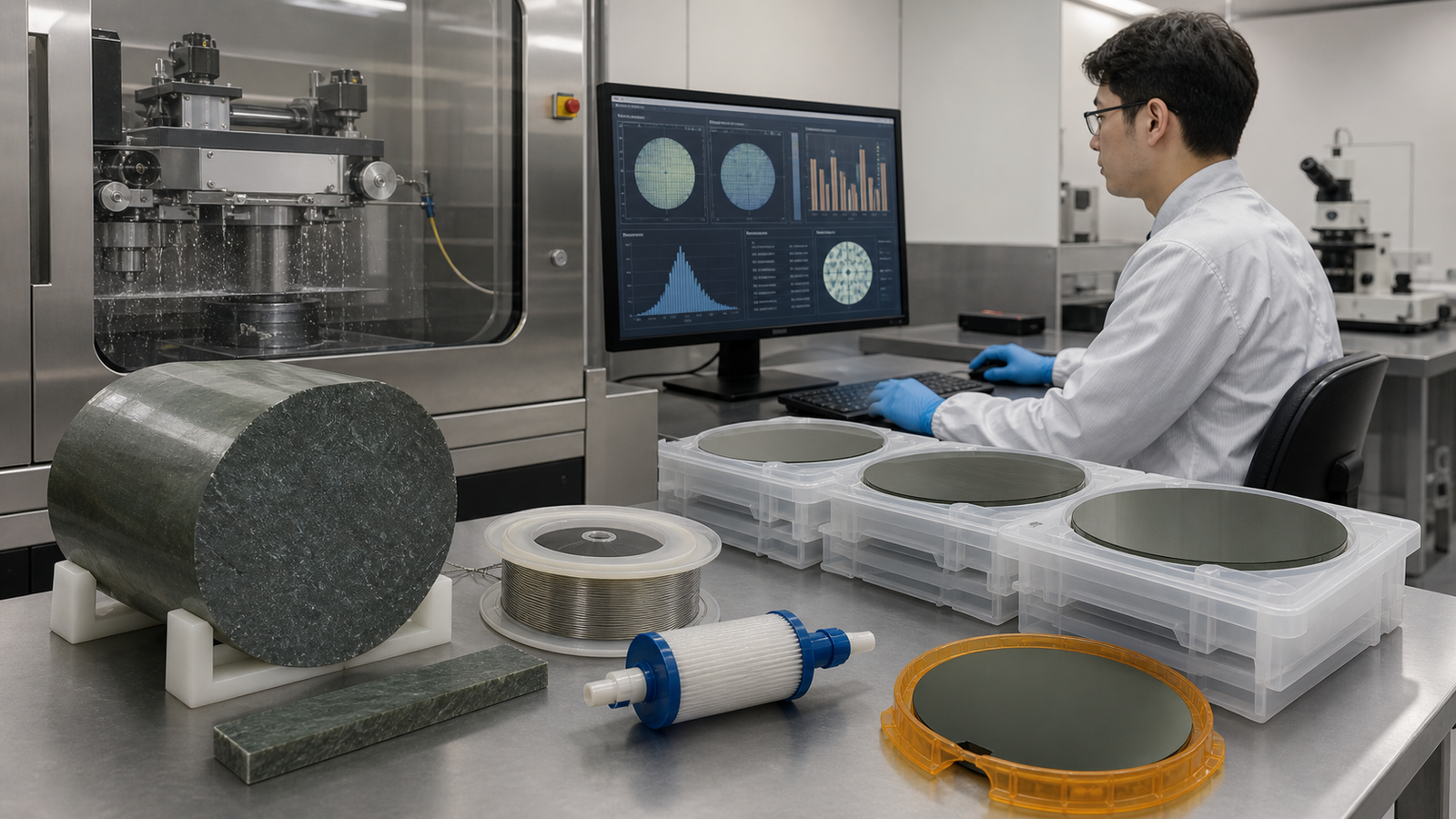
The Precision Optical Wafer Processing systems are specially designed for optical wafer slicing, LED sapphire substrate dicing, and photonic crystal wafer processing. For these applications, ewirexon offers configuration options with high-precision multi-wire saws as well as single-wire cutting units. Both options feature an extremely stable, vibration-damped steel frame design. The multi-wire system achieves very high production efficiency (high volume, ultra-low kerf loss) in a compact footprint, while the single-wire unit delivers superior dimensional accuracy for thin wafers. Both options integrate seamlessly into automated wafer processing lines and can be swapped depending on production requirements, enabling ideal alignment to customer-specific manufacturing workflows with minimal setup changes.
| NO. | パラメータ | 仕様 |
| 1 | モデル | TCQF600PNC |
| 2 | 切断の原理 | Endless diamond wire / Physical cutting |
| 3 | Cutting Functions | Flat Cutting / Rotary Slicing |
| 4 | Maximum Workpiece Size(mm) | 200 × 200 × 220 mm (L×W×H) |
| 5 | Worktable Size(mm) | Ø600 转台 |
| 6 | Cutting Planarity Accuracy(mm) | 0.1 |
| 7 | Surface Roughness(μm) | Ra 0.8 μm |
| 8 | Wire Specification(mm) | 0.65–1.0/3720 |
| 9 | テンションシステム | Constant Wire Tension Control |
| 10 | ガイドホイールの数量 | 3つの車輪 |
| 11 | 駆動モーター | Servo motor |
| 12 | Wire Speed (m/s) | 51Max(Adjustable) |
| 13 | Total Power | 3.3 |
| 14 | Voltage | 380v 50Hz |
| 15 | 制御システム | Custom-developed Tongcheng T30 system |
| 16 | Footprint (L×W×H)(mm) | 1650×1750×2010 |
| 17 | Gross Weight kg | 1250 |

ダイヤモンドワイヤーソーがガラスコア基板の研究開発においてどのような役割を果たすのか、エッジの損傷をどのように抑制するのか、また、レーザーやブレードによる個片化のどちらが適しているのかについて学びましょう。.

ダイヤモンドワイヤーソーを用いたNdFeB磁石の切断において、波打ち、欠け、ワイヤーの摩耗、および材料の損失を抑制する方法について、測定可能な試作計画を通じて学びましょう。.

試行錯誤によるパラメータ変更ではなく、ワイヤ経路、張力、負荷、冷却液、摩耗、および固定具の状態といった証拠に基づいて、ダイヤモンドワイヤーソーの破損原因を診断する。.

AlN基板の切断におけるダイヤモンドワイヤーソー加工の適格性評価方法、チッピングや表面下損傷の抑制方法、および実験用・量産用装置の選定方法について学びます。.

ダイヤモンドワイヤーソー技術が、半導体パッケージング、パワーエレクトロニクス、および精密部品向けの先端セラミック切断をどのように向上させるかをご覧ください。.

ダイヤモンドワイヤーソー技術が、LED、RF、光学、半導体用途におけるサファイア基板の切断をどのように改善するかについてご紹介します。.
ewirexon.com
通常、数分以内に返信があります
こんにちは。何かお手伝いできることはありますか?
WhatsAppでメッセージを送る
🟢オンライン | プライバシーポリシー
WhatsAppでメッセージを送ってください