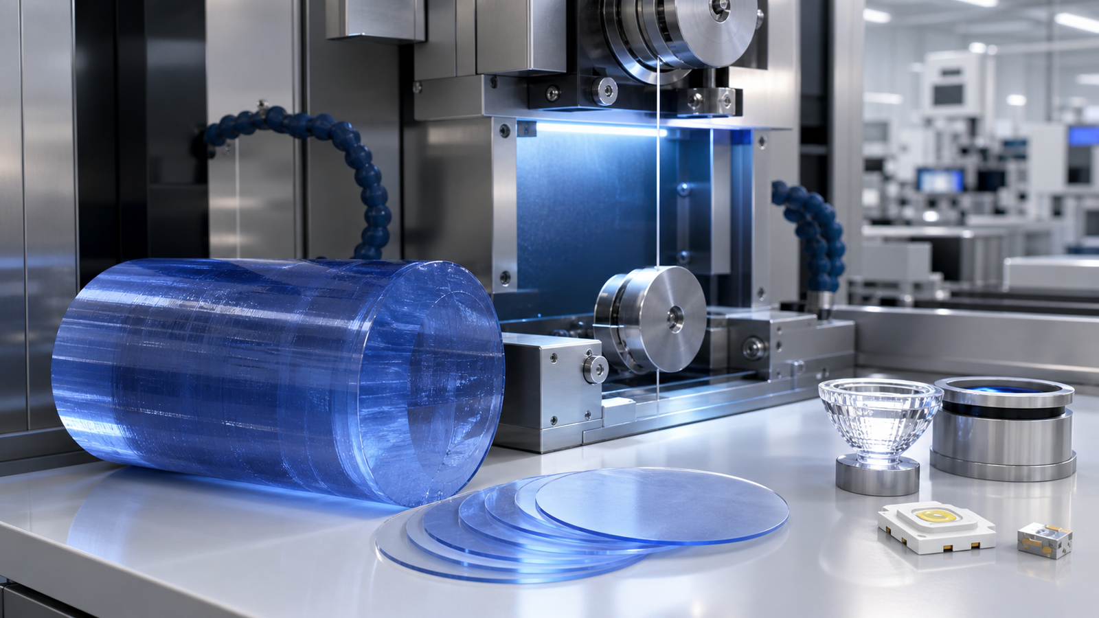









PCB基板材料のスライス加工


High-Precision Wire Saw Systems for Electronic Substrate Processing

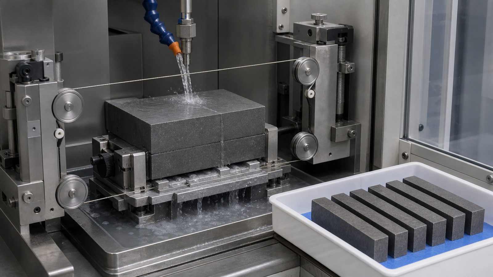
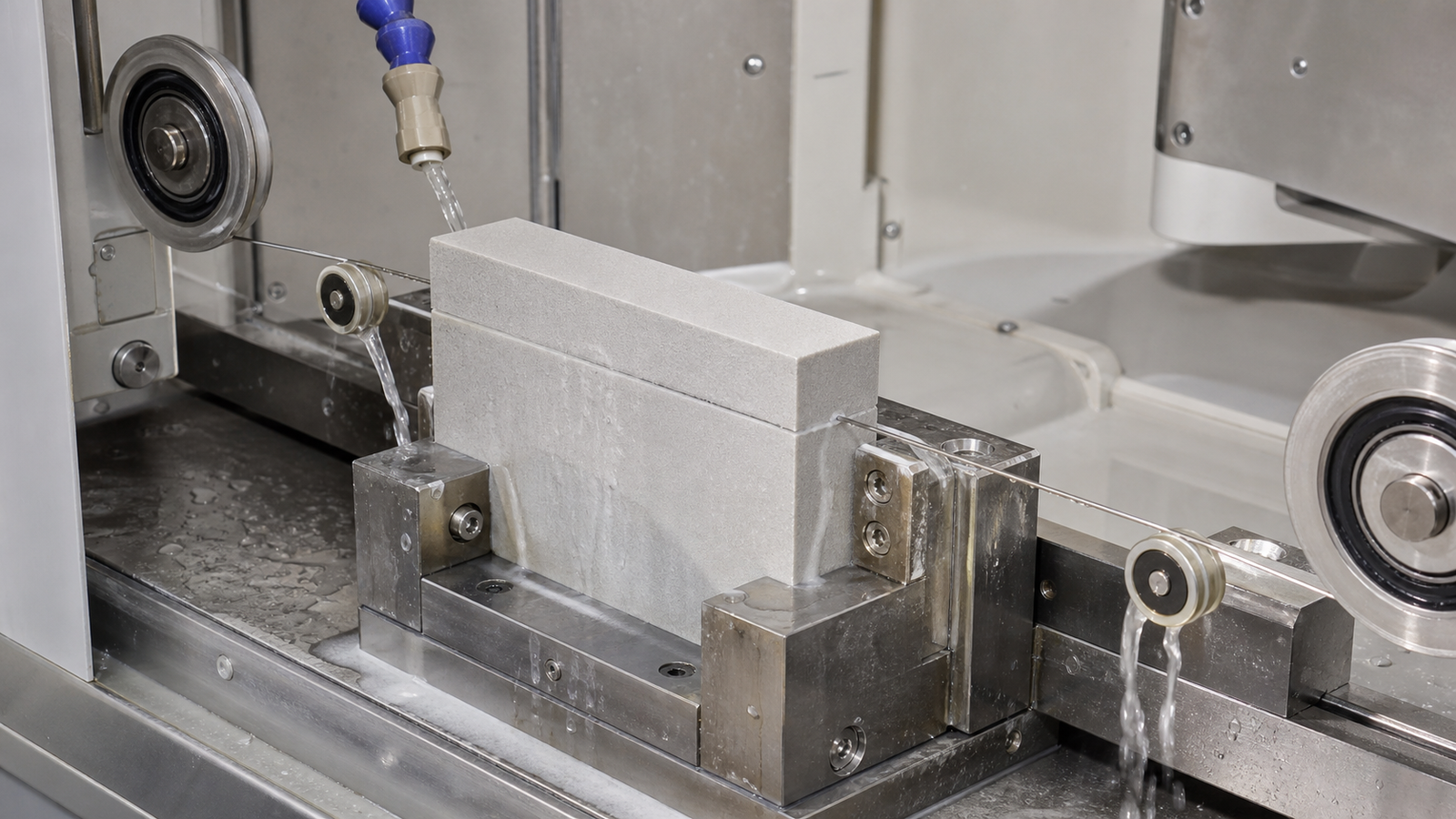
Rigid, flexible, and rigid-flex circuit substrates form the backbone of electronic devices, from consumer gadgets to industrial control systems. Precision slicing of these substrates is essential to maintain circuit integrity, flatness, and electrical performance. Diamond wire cutting provides a damage-free alternative to traditional methods, preserving substrate properties and eliminating delamination.

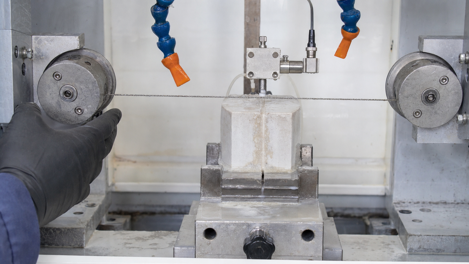
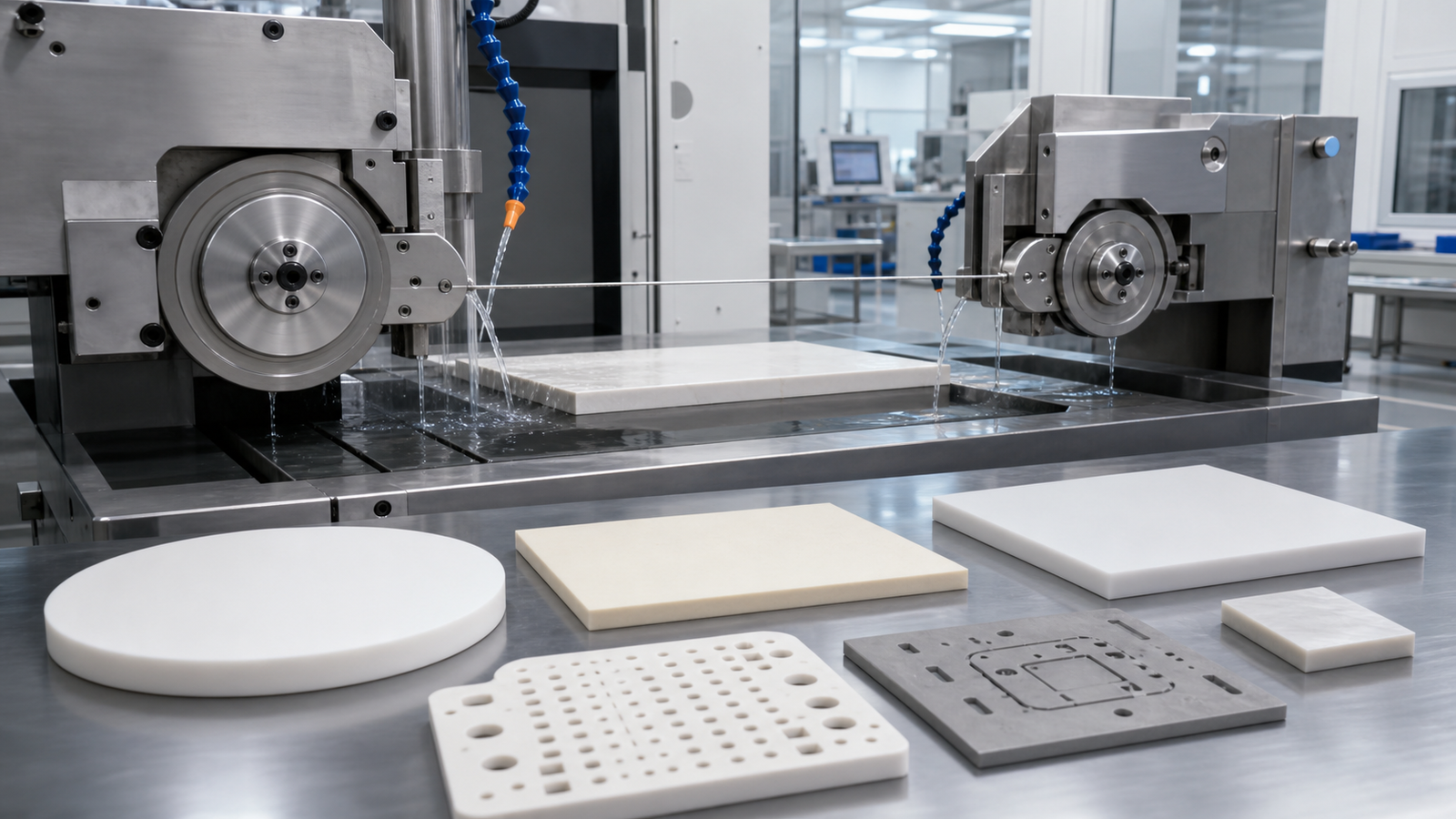
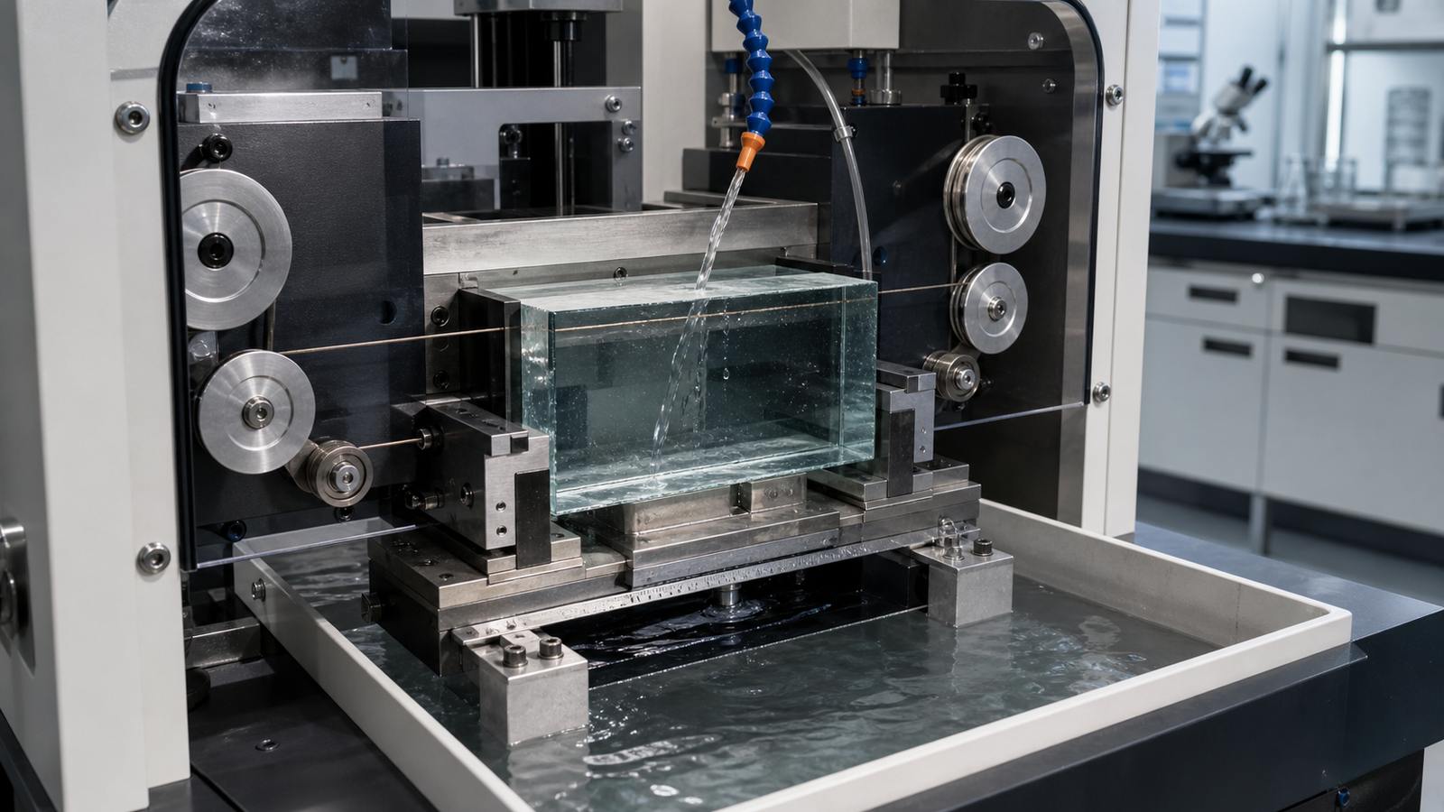
Our specialized systems deliver precise, clean slicing for FR-4, ceramic, polyimide, and copper-clad laminates, ensuring consistent thickness and flatness across large-format panels. The closed-loop tension control and real-time monitoring prevent micro-cracks and fiber damage, critical for high-density, fine-pitch circuit boards.

Suitable for both R&D prototyping and mass production, our solutions support high-throughput processing for multi-layer PCBs and advanced circuit substrates. The intelligent CNC control allows for precise parameter adjustment, ensuring compatibility with the latest PCB technologies and flexible circuit manufacturing processes.

Precision Slicing Systems for PCB & Circuit Substrates


Our diamond wire cutting solutions are tailored for high-precision slicing of rigid, flexible, and rigid-flex PCB base materials, ceramic substrates, and semiconductor packaging substrates. The systems feature closed-loop tension control and real-time monitoring, ensuring consistent thickness, flatness, and damage-free cutting for high-density, fine-pitch circuit boards. This eliminates delamination and micro-cracks, directly improving PCB yield and reliability in mass production.

回路基板とPCB基材のスライス

メリット
  • Damage-Free Processing: Prevents substrate delamination and fiber damage, critical for high-frequency PCB performance.
  • Consistent Thickness Control: Maintains uniform substrate thickness across large panels, ensuring stable circuit etching.
  • High Compatibility: Supports a full range of substrate materials, including FR-4, ceramic, polyimide, and copper-clad laminates.
  • High-Efficiency Mass Production: Multi-wire cutting design reduces processing time per panel, lowering production costs.
  • PCB base material slicing for consumer and automotive electronics
  • Ceramic substrate cutting for semiconductor packaging and power modules
  • Flexible circuit substrate processing for wearable and 5G devices
NO.パラメータ仕様
1モデルTCQF400LNC-FM-HL
2切断の原理エンドレス・ダイヤモンドワイヤー/物理的切断
3切断機能スライス加工/角度・形状切断
4最大ワークサイズ(mm)Φ600mm、高さ500mm
5作業台のサイズ(mm)Ø380 转台
6切断平面度精度(mm)0.08
7表面粗さ(μm)Ra 0.8μm
8ワイヤの仕様(mm)Ø0.65–1.0/2580
9テンションシステムワイヤ張力の恒常制御
10ガイドホイールの数量4輪
11駆動モーターサーボモーター
12ワイヤ速度(m/s)51Max(調整可能)
13総出力(kW)2.8
14電圧220V 50Hz
15制御システム特注開発のTongcheng T32システム
16外形寸法(長さ×幅×高さ)(mm)1350×1066×1968
17総重量(kg)720
0

Read the Case: Improve PCB Base Material Slicing Quality

Professional PCB base material slicing enterprises adopted our solutions to upgrade equipment and workflows, gaining higher yield, lower waste and reliable slicing precision.
当社の技術事例について詳しく知りたい方は、ぜひお問い合わせください。.

お問い合わせ

2D図面と、少なくとも1つの3D CADファイルをアップロードいただくと、より迅速かつ正確な見積もりをご提供できます。ファイルが複数ある場合は、.zipまたは.rar形式で圧縮してください。メールでのご連絡をご希望の場合は、info@xxx.com までお見積り依頼(RFQ)をお送りください。.

ニュース&最新情報