
An as-cut surface can look smooth and still contain cracks below the surface. Those cracks become important later: grinding can open them, polishing can reveal pits, cleaning can enlarge them, and thermal or mechanical loading can turn them into fractures. This hidden layer is subsurface damage (SSD).
For SiC, silicon, sapphire, quartz and advanced ceramics, SSD connects slicing to every downstream finishing step. If the allowance is too small, damage remains in the product. If it is too large, expensive material, time and consumables are wasted. A हीरे की तार वाली आरी should therefore be evaluated by the finishing stock required for stable final quality, not surface roughness alone.
This guide presents a practical way to build an SSD and stock-removal budget, choose measurements and use the result for process optimization and equipment acceptance.
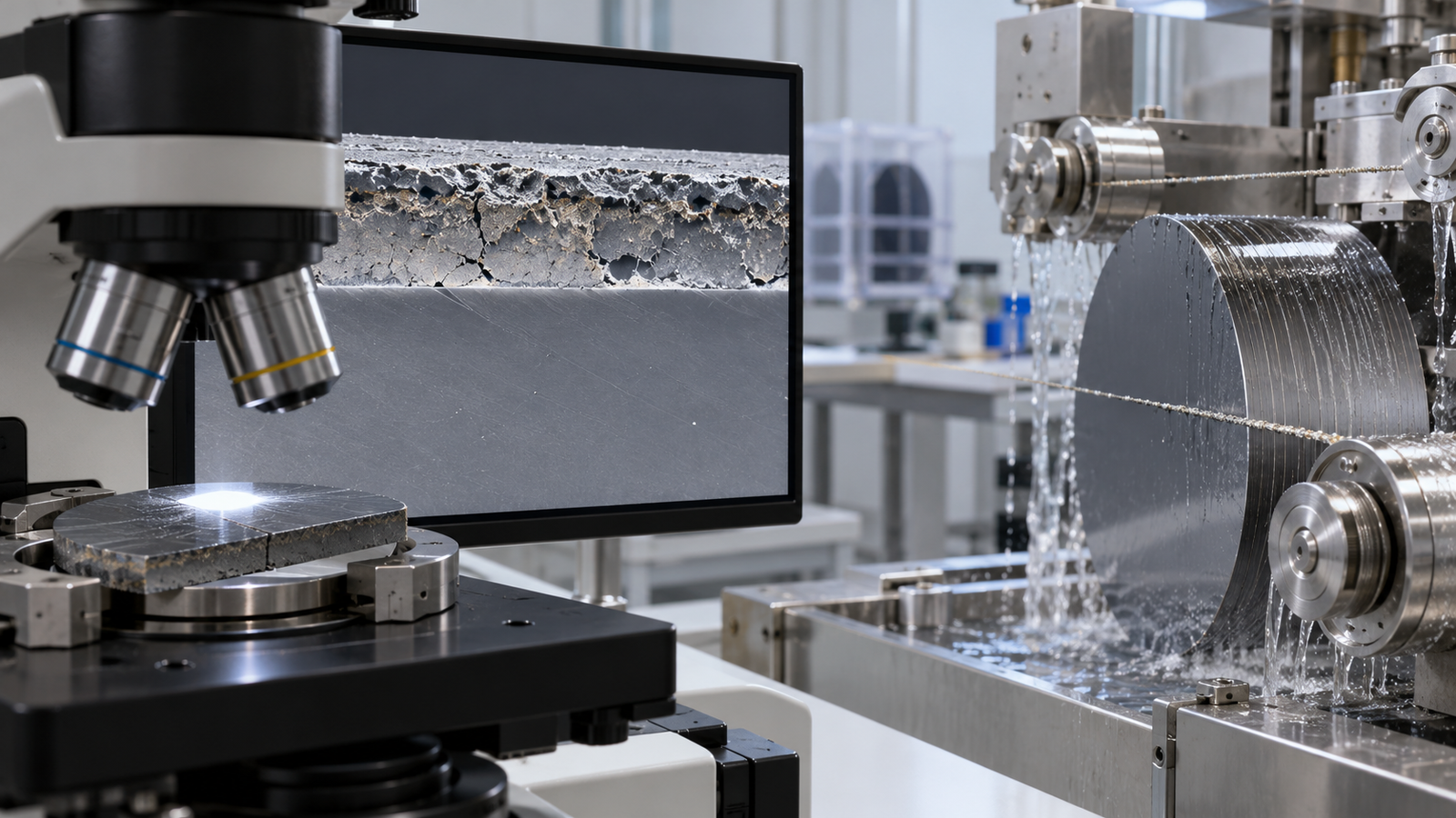
What subsurface damage includes
Fixed diamond grains remove brittle materials through a combination of ductile deformation, microcutting, ploughing and brittle fracture. The resulting affected zone can contain median and lateral cracks, crushed material, residual stress, phase changes or dislocations depending on the material and cutting conditions.
SSD is not one universal boundary. Different methods respond to different features. A chemical etch may reveal cracks that a polished cross-section misses, while spectroscopy can identify stress or phase change without measuring every crack. The specification should state what damage is being measured and why it matters to the next process.
For production control, distinguish:
- surface topography: roughness, grooves and waviness visible at or above the surface;
- fracture damage: cracks and chipped zones extending below the cut face;
- stress or structural change: altered material not captured by a simple crack-depth value;
- contamination: embedded particles or residues that may accompany damage but require separate measurement.
Why roughness cannot stand in for SSD
Ra, Sa and related roughness parameters are useful process signals, but they describe surface height statistics over a defined filter and area. Two surfaces can share a similar Ra and have different crack depth. A worn wire may create a superficially smoother rubbed surface while force and subsurface damage rise.
Research has explored statistical relationships between roughness features and damage depth, but such models require calibration for the material, process and measurement method. Use roughness as a rapid monitor after a correlation study, not as an assumed universal conversion.
Waviness should also be separated from roughness. Long-period wire deflection or vibration can drive grinding stock even when local roughness is acceptable. Preserve both profiles and the wire-travel direction.
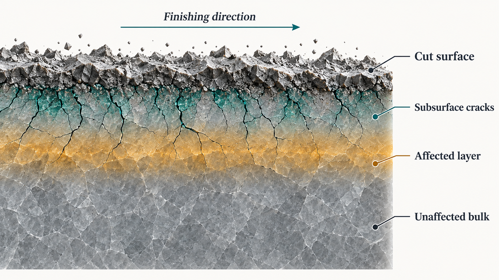
Methods for measuring the damaged layer
Cross-sectioning and microscopy
A section through the cut face can reveal cracks under optical or electron microscopy. Preparation must avoid creating or smearing damage. Examine enough length and several positions because the deepest crack, not the average, can control the safe allowance.
Controlled polishing or layer removal
Remove known thickness increments and inspect when damage indicators disappear. This directly links SSD to finishing allowance but consumes samples and requires accurate material-removal measurement. It is valuable for process qualification.
Etching techniques
Material-specific etches can open or reveal cracks. The chemistry, time and temperature must be controlled because etching changes feature size. Use suitable safety and contamination controls and do not transfer an etch method between silicon, SiC, sapphire and glass.
Spectroscopic and non-destructive methods
Raman, X-ray and acoustic or optical techniques can map stress or structural change. They may not directly measure every fracture. Validate the signal against a destructive reference before using it for release.
Build a finishing-allowance budget
A finishing budget starts from the final accepted thickness and works backward. Include removal needed for three different purposes:
- Geometry correction. Stock needed to remove TTV, taper, bow-related contact variation and waviness.
- Damage removal. Stock needed to pass below the qualified SSD distribution with a safety margin.
- Final surface generation. Stock consumed by lapping, polishing, texturing or other finishing steps to meet functional roughness and cleanliness.
Do not simply add the maximum value from every process. Some removal occurs simultaneously. Build a step-by-step material balance using actual incoming and outgoing thickness maps. Preserve uncertainty and process variation.
For double-sided finishing, define how removal is split between faces. If one cut face has deeper damage or larger waviness, an equal-removal assumption may leave damage on one side while over-processing the other.
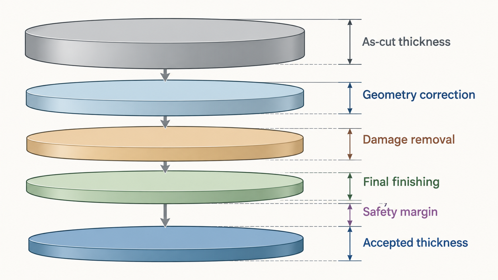
An example budgeting workflow
Consider a brittle wafer that must finish at a specified thickness. Start with the final lower thickness limit. Add the planned polishing and lapping removal, then add the geometry and SSD allowance derived from capability data. Add a process safety margin based on measurement uncertainty and lot variation. The result establishes the target as-cut thickness.
The budget should answer:
- Which step removes the deepest observed saw damage?
- How much stock remains before the final thickness lower limit?
- Does a high-TTV wafer consume the SSD safety margin?
- Are edge exclusion and center regions budgeted separately?
- How does later wire life change required removal?
- What is the material and cycle-time cost of each extra micrometer?
Use distributions, not one “typical” wafer. A budget that works for the mean and fails the 95th-percentile damage depth will create intermittent downstream loss.
How cutting parameters affect SSD
SSD is influenced by grain penetration and uncontrolled crack growth. Higher feed per active grain generally raises load. Wire speed changes the number of abrasive engagements and heat. Tension affects bow and dynamic stability. Abrasive size, protrusion and bond determine contact severity and chip space. Coolant affects friction, temperature and debris recutting.
A 2025 optimization study on polycrystalline silicon reported smoother surfaces and shallower SSD at a lower feed-to-wire-speed ratio within its tested range. That is useful evidence of a ratio effect, not a universal recipe. Material microstructure, wire and equipment determine the usable window.
Design experiments around physically meaningful variables. Record feed per contact length, wire exposure and coolant state. Change one factor at a time during early diagnosis, then use a structured multivariable design once the stable region is known.
Wire wear changes the damage budget
A fresh wire, conditioned wire and late-life wire do not interact with the material the same way. Blunting can raise force; grain pull-out can reduce active density; loose particles can recut the surface. A machine acceptance test performed only with a selected fresh wire understates production variation.
Sample SSD at defined exposure stages. Track cut area, wire travel or new-wire consumption rather than time alone. Link damage data with force, drive load, cycle time and surface metrics. The diamond wire wear guide explains how to create replacement limits before quality drifts.
Use SSD to compare cutting technologies
When comparing an endless diamond wire saw, diamond multi-wire saw, blade, laser or other process, normalize the endpoint. One process may cut faster but require more grinding; another may have a wider kerf but less damage. Compare total material loss, finishing time, consumables and accepted yield.
| Measure | Why it belongs in the comparison |
|---|---|
| Geometric kerf | Direct loss during separation |
| TTV and waviness | Stock needed for geometry correction |
| SSD distribution | Stock needed to remove hidden damage |
| Edge damage | Usable area and breakage risk |
| Finishing cycle and consumables | Downstream cost |
| Final accepted yield | Economic result |
A production control plan
SSD measurement can be slow, so use a tiered plan. Perform destructive or high-detail methods during qualification and after major changes. Correlate them with faster roughness, force, power, wire-life and geometry indicators for routine monitoring. Reconfirm the correlation at a defined interval.
Trigger a deeper study after a wire supplier change, new material grade, diameter change, guide replacement, coolant change, major maintenance or unexplained finishing loss. Retain samples and raw profiles so historical drift can be reviewed.
The site’s surface-quality inspection guide shows how metrology can feed parameter control instead of becoming an end-of-line report.
How ewirexon supports damage and allowance trials
Ewirexon develops endless diamond wire saw and diamond multi-wire saw solutions for SiC, silicon, sapphire, quartz, glass, graphite and ceramics. A useful trial package includes the material grade and orientation, dimensions, final thickness, surface and edge specification, finishing sequence, metrology methods and production objective.
A sample cutting trial can produce mapped coupons for destructive SSD analysis and finishing tests. The equipment decision can then use total kerf-plus-finishing loss and accepted yield, rather than relying on one roughness number.
निष्कर्ष
Subsurface damage is the hidden link between diamond wire saw cutting and final product quality. Ignoring it risks latent cracks; overestimating it wastes valuable SiC, silicon, sapphire, quartz or ceramic.
Define what damage matters, validate the measurement, and build a stock-removal budget from the final thickness backward. Correlate detailed SSD checks with faster production signals and repeat them across wire life. That creates a realistic allowance, a fair equipment comparison and a clearer route to lower total material loss.
अक्सर पूछे जाने वाले प्रश्न
What is subsurface damage in diamond wire saw cutting?
It is the layer below the cut surface containing cracks, deformation, residual stress or structural change caused by abrasive removal.
Can surface roughness predict SSD depth?
Only after a material- and process-specific correlation study. Similar roughness values can hide different crack depths, especially as wire wear changes.
How is subsurface damage measured?
Methods include prepared cross-sections, controlled layer removal, material-specific etching, microscopy and calibrated spectroscopic or non-destructive techniques.
How much finishing allowance is needed?
It must cover geometry correction, the qualified SSD distribution, final surface generation and uncertainty while preserving the final thickness limit.
Does lower feed always reduce subsurface damage?
Lower grain load can help within a stable range, but excessive rubbing, wire wear or poor debris removal can offset the benefit. Qualify feed together with wire speed and contact length.
तकनीकी संदर्भ
- Review of SiC surface and subsurface damage and finishing processes, 2026.
- Optimization of diamond-wire-sawn polycrystalline silicon surface and SSD, 2025.
- Prediction of subsurface damage from surface-topography features.
- Microstructure and damage of diamond-wire-sawn monocrystalline silicon, 2025.
Editorial note: SSD definitions and safe allowances are material- and application-specific. The figures are AI-generated engineering illustrations, not certified microscopy or customer data.