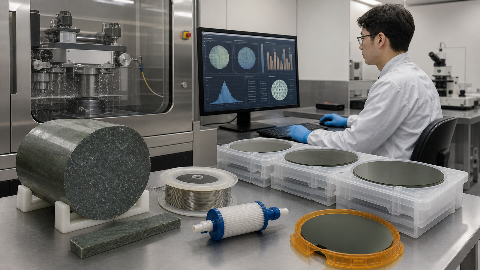









Solución para el corte de obleas fotovoltaicas


Precision Diamond Wire Cutting for Solar Wafer Production

High-efficiency N-type and P-type solar wafers are the core of next-generation photovoltaic modules. Precision diamond wire cutting is critical to producing ultra-thin, high-quality wafers that maximize cell conversion efficiency and material yield. This process has replaced traditional sawing, delivering lower kerf loss, higher throughput, and superior surface quality for mass PV manufacturing.

Our diamond wire systems ensure consistent wafer thickness, minimal breakage, and controlled surface damage, enabling high-throughput production of ultra-thin wafers while meeting the strict quality requirements of modern solar cell technologies.

Precision Diamond Wire Cutting for High-Efficiency Solar Wafers

Our diamond wire cutting solutions are tailored for high-efficiency PV wafer production, delivering ultra-thin, high-quality wafers that directly boost solar cell conversion efficiency. The systems feature advanced wire path optimization and real-time monitoring, ensuring consistent thickness, flatness, and surface quality for N-type TOPCon, HJT, and other next-generation solar cells. With low-damage cutting technology, they minimize wafer warpage and micro-cracks, significantly improving cell yield and module performance.

Procesado de obleas fotovoltaicas de alta eficiencia

Core Benefits
  • Ultra-Thin Wafer Capability: Achieve stable slicing of wafers as thin as 100μm, reducing silicon usage and lowering cell costs.
  • Superior Surface Quality: Low-damage cutting eliminates the need for extensive post-processing, simplifying production steps.
  • High Yield & Low Breakage: Intelligent cutting algorithms reduce wafer breakage rate to below 1%, maximizing production yield.
  • Energy & Cost Savings: High-efficiency cutting design reduces power consumption per wafer, cutting operational expenses.
  • High-efficiency N-type/P-type solar wafer manufacturing
  • Ultra-thin wafer processing for HJT, TOPCon, and IBC cells
  • Wafer slicing for bifacial and high-power PV modules
N.º.ParámetroEspecificaciones
1ModeloTCQF15030CNC
2Principio de corteAlambre de diamante sin fin / Corte físico
3Funciones de corteCorte / Corte de contornos en 2D
4Tamaño máximo de la pieza de trabajo (mm)1200 × 1000 × 1000 mm (largo × ancho × alto)
5Dimensiones de la mesa de trabajo (mm)1500×300
6Precisión de planitud del corte (mm)0.1
7Rugosidad superficial (μm)Ra 0,8 μm
8Especificaciones del alambre (mm)Ø 0,65–1,0/6250
9Sistema de tensiónControl de tensión constante del cable
10Cantidad de ruedas guía4 ruedas
11Motor de accionamientoServomotor
12Velocidad del alambre (m/s)51Max (ajustable)
13Total Power3.6
14Tensión220 V, 50 Hz
15Sistema de controlSistema Tongcheng T33 desarrollado a medida
16Dimensiones (L × An × Al) (mm)3200×1500×1500
17Peso bruto (kg)3200
12

Case Learning: Enhance PV Wafer Processing Efficiency

Our cooperation in high-efficiency PV wafer processing optimized production lines, resulting in higher yield, lower material consumption and sustained processing precision.
¿Quieres saber más sobre nuestros casos técnicos? Ponte en contacto con nosotros.

¡Escríbenos!

Sube tus planos en 2D y al menos un archivo CAD en 3D para obtener un presupuesto más rápido y preciso. Si tienes varios archivos, comprímelos en un archivo .zip o .rar. ¿Prefieres el correo electrónico? Envía tu solicitud de presupuesto a info@xxx.com.

Noticias