






SiC 및 화합물 반도체 절단


High-precision Diamond Wire Cutting Systems for Substrate Slicing

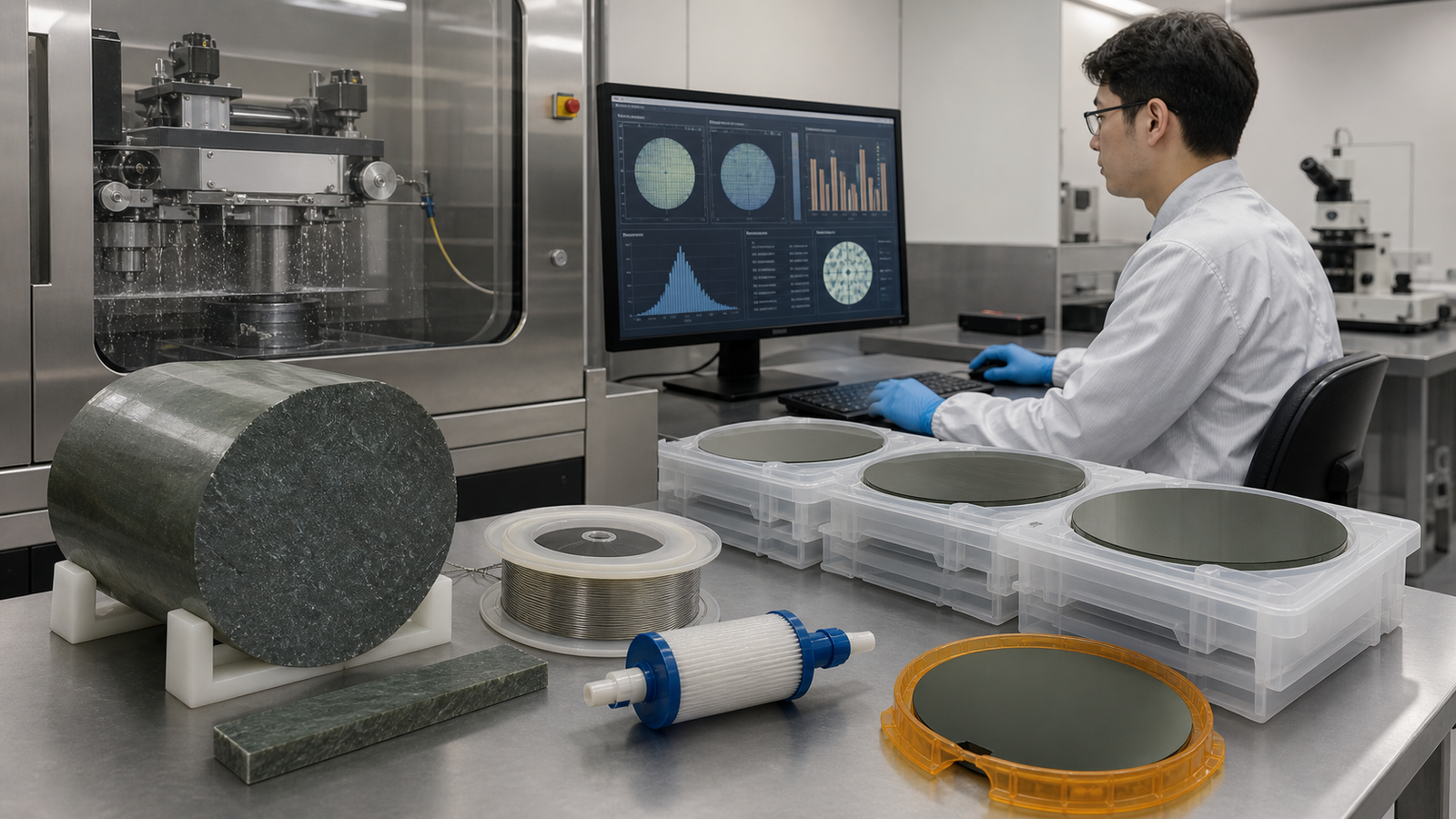
SiC ingots, compound semiconductor substrates and wide-bandgap materials experience significant mechanical stress and thermal impact during high-speed slicing. To ensure excellent surface quality, minimal sub-surface damage and avoid chipping or micro-cracks that lead to device failure, semiconductor manufacturers require highly stable cutting processes and precise process control. This is the only way to achieve reliable, high-yield production of high-quality wafers.

Processing SiC and compound semiconductors involves extremely high material and production costs. Around 30% of total substrate manufacturing cost comes from inefficient cutting, material loss and low yield, rather than raw materials alone. Choosing the right diamond wire cutting systems for specific applications can therefore greatly reduce production costs and improve efficiency.

High-precision diamond wire saws are used to slice hard, brittle ingots into thin wafers with stable tension and feed control. Their operating parameters are optimized for a stable process window with consistent wire tension, low vibration and narrow kerf width.

SiC 및 화합물 반도체 공정

ewirexon SiC & Compound Semiconductor Diamond Wire Cutting System

The new SiC & Compound Semiconductor diamond wire cutting systems from ewirexon are specially developed for high-precision slicing of SiC ingots and wide-bandgap substrates, where ultra-high wafer yield and minimal surface damage are required. The new SiC Series achieves significantly higher material yield than competitor products in this application area. The use of our cutting systems enables savings in production costs for semiconductor fabs. Another positive side effect is the reduction of material waste and surface damage.

  • Potential savings in production costs through higher material yield of the cutting systems in typical SiC processing lines
  • 자원의 최적 활용
  • 절단 손실과 표면 하부 손상을 최소화함으로써 생산 과정에서 자재 비용을 절감할 수 있습니다.
  • 모듈식 구조와 작은 설치 면적 덕분에 유연하고 컴팩트한 장비 설계가 가능합니다.
  • 사용자 친화적인 조작 방식과 원격 모니터링 기능 덕분에 설치 및 유지보수 시 작업이 더욱 수월해집니다.
  • 다이아몬드 와이어 및 기계 부품의 수명 연장을 통한 유지보수 비용 절감
  • 맞춤형 공정 매개변수와 완벽한 시스템 통합을 통해 경제적인 턴키 시스템 솔루션을 제공합니다.
  • SiC 및 화합물 반도체 공정
  • Power Semiconductor Wafer Manufacturing
  • Ingot Slicing & Substrate Processing
  • Wide-Bandgap Material Cutting
  • 연구개발(R&D) 실험실 및 시범 생산 라인
  • Advanced Packaging Facilities
아니요.매개변수사양
1모델TCQF400LNC-FM-HL
2절단 원리무한 다이아몬드 와이어 / 물리적 절단
3절단 기능슬라이싱 / 각도 및 단면 절단
4최대 공작물 크기(mm)Φ600mm, 높이 500mm
5작업대 크기(mm)Ø380 转台
6절단 평탄도 정밀도(mm)0.08
7표면 거칠기(μm)Ra 0.8μm
8와이어 사양(mm)Ø0.65–1.0/2580
9장력 시스템일정한 와이어 장력 제어
10가이드 휠 수량4륜
11구동 모터서보 모터
12와이어 속도 (m/s)51Max(조절 가능)
13총 출력(kW)2.8
14전압220V 50Hz
15제어 시스템맞춤 개발된 통청 T32 시스템
16치수 (길이×폭×높이)(mm)1350×1066×1968
17총 중량 (kg)720
2

Case Study: SiC & Compound Semiconductor Processing

This case study shows how the optimal selection of ewirexon diamond wire cutting systems can help boost wafer yield for SiC & compound semiconductor processing by up to 15% and thus sustainably lower the production costs of power semiconductor fabs. In addition, ewirexon’s SiC slicing solution delivers minimal surface damage, reduced material waste and higher production throughput compared to conventional cutting methods.

더 많은 프로젝트 사례를 알고 싶으신가요? 언제든지 저희에게 연락해 주세요!

문의해 주세요!

더 빠르고 정확한 견적을 받으시려면 2D 도면과 3D CAD 파일 1개 이상을 업로드해 주세요. 파일이 여러 개인 경우, .zip 또는 .rar 파일로 압축해 주시기 바랍니다. 이메일을 선호하시나요? 견적 요청(RFQ)을 info@xxx.com으로 보내주세요.

뉴스 및 업데이트