





전자용 세라믹 기판 절단


Diamond Wire Cutting Systems for Electronic Ceramic Substrate Manufacturing & Dicing

Electronic ceramic substrates are used in a wide variety of semiconductor and electronic manufacturing processes. Without sufficient precision cutting, the dimensional errors and material damage generated during substrate processing can lead to reduced device performance, increased yield loss and consequential failure of the end product. To ensure optimum functionality of multi-layer ceramic components, power modules and electronic packages at all times and to minimize production downtime, reliable, high-precision substrate processing must be ensured.

In addition to ultra-tight dimensional accuracy to meet the packaging requirements, the diamond wire cutting systems used should meet other requirements. Among other things, semiconductor industry quality standards must be complied with, which means that the cutting systems must have very low kerf loss and minimal sub-surface damage. Furthermore, there are high requirements for process stability, for example when used in high-volume production lines, so the systems must be designed so that there is consistent, repeatable cutting performance. In addition, a compact footprint is of great importance when integrated into automated substrate manufacturing lines with limited factory space.

ewirexon Electronic Ceramic Substrate Processing

Electronic Ceramic Substrate Cutting Systems

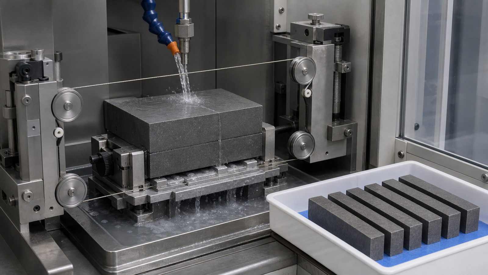
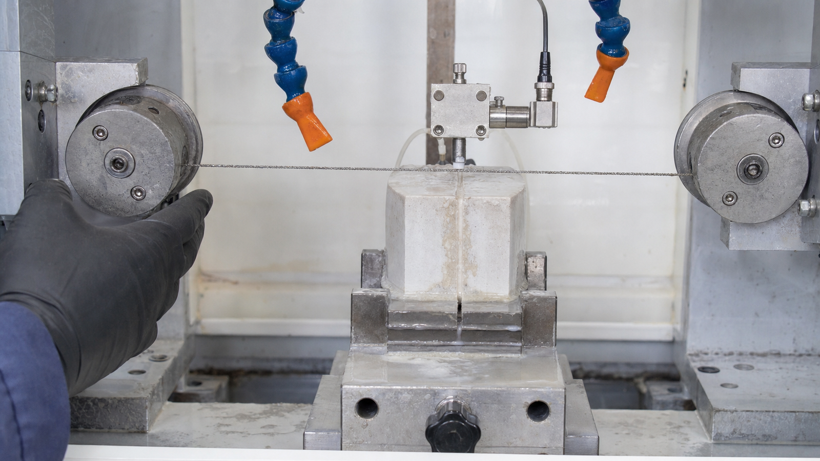
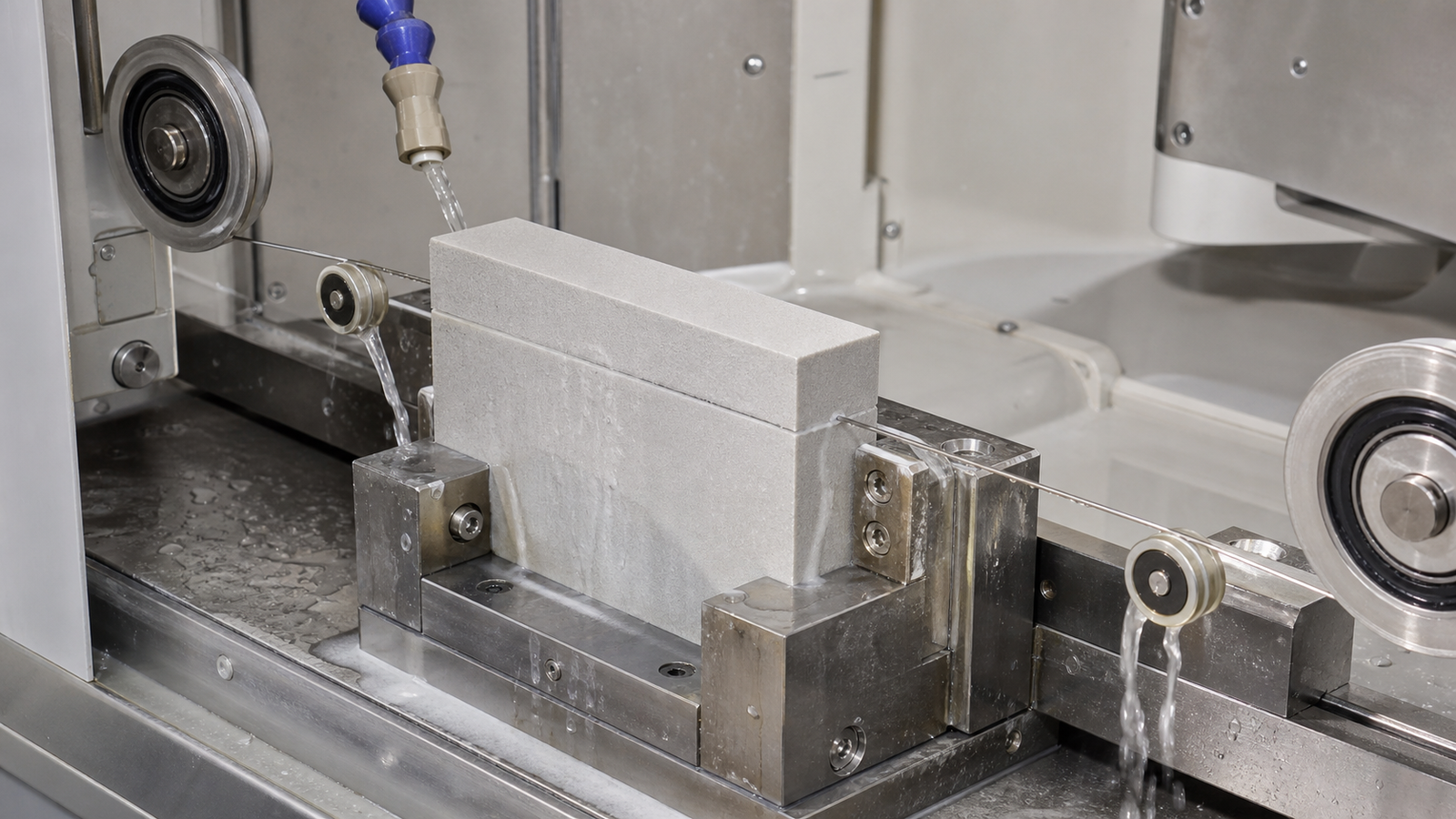
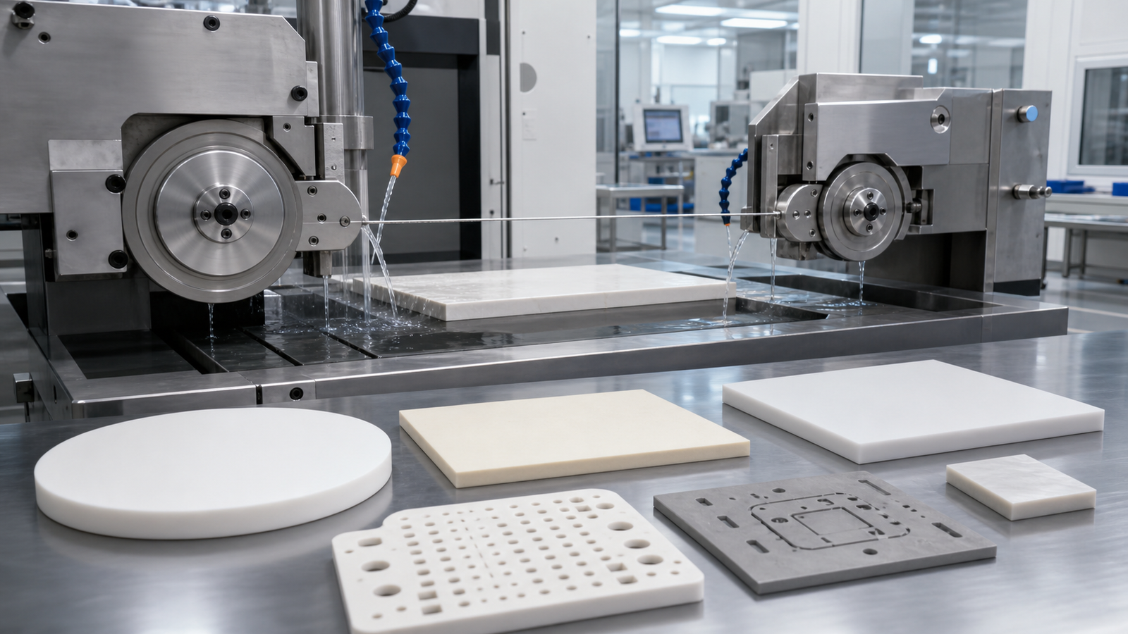
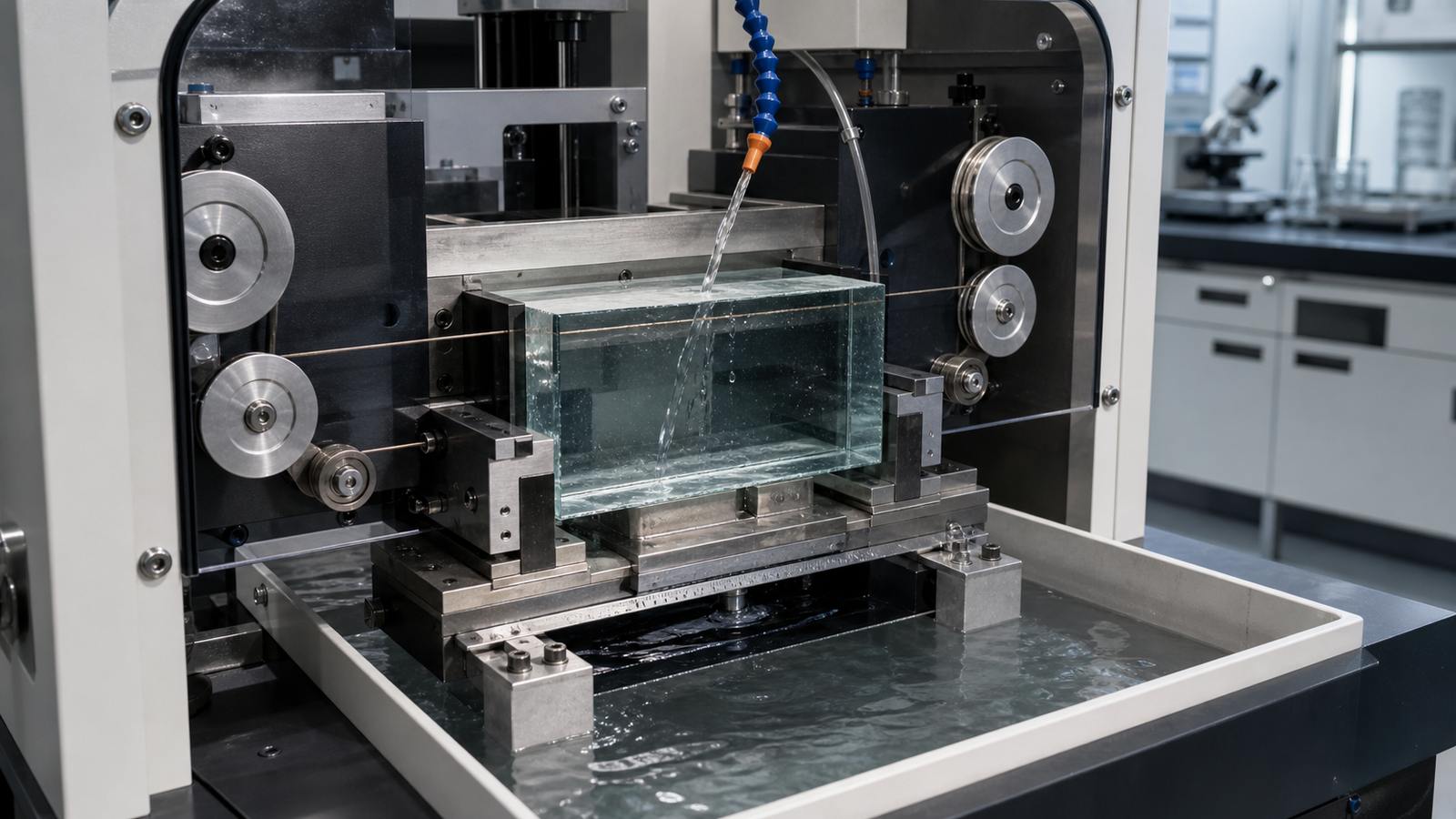
With the Electronic Ceramic Substrate Processing Line, ewirexon supplies some of the world’s most high-precision and at the same time most cost-effective diamond wire cutting systems for electronic ceramic substrate manufacturing. Specially developed for slicing alumina, aluminum nitride (AlN) and multi-layer ceramic substrates, the cutting systems deliver ultra-tight dimensional accuracy with a very compact and robust design. Thus, the systems enable a space-saving production line design even at high throughput and variable processing parameters. Thanks to the low kerf loss of the cutting systems, material yield can be maximized depending on the substrate type.

  • Easier maintenance and assembly
  • thanks to modular, user-friendly system design.
  • Favors space-saving production line design
  • as the particularly compact cutting systems allow for a streamlined layout of the overall manufacturing cell.
  • Competitive advantage due to cost savings
  • as the highly efficient cutting process allows the use of standard production lines without costly custom modifications, maximizing material yield and reducing waste.
  • Avoidance of downtimes / low wear
  • The robust design of the cutting system allows it to be used even at high speeds and in continuous 24/7 production environments.
  • Short delivery times, low transport costs.
  • Electronic ceramic substrate slicing & dicing
  • Processing of AlN, alumina and multi-layer ceramic substrates
  • High-precision cutting for power electronic packages
  • Substrate manufacturing for semiconductor components
  • Ceramic component processing for electronic devices
아니요.매개변수사양
1모델TCQF400LNC-FM-HL
2절단 원리무한 다이아몬드 와이어 / 물리적 절단
3절단 기능슬라이싱 / 각도 및 단면 절단
4최대 공작물 크기(mm)Φ600mm, 높이 500mm
5작업대 크기(mm)Ø380 转台
6절단 평탄도 정밀도(mm)0.08
7표면 거칠기(μm)Ra 0.8μm
8와이어 사양(mm)Ø0.65–1.0/2580
9장력 시스템일정한 와이어 장력 제어
10가이드 휠 수량4륜
11구동 모터서보 모터
12와이어 속도 (m/s)51Max(조절 가능)
13총 출력(kW)2.8
14전압220V 50Hz
15제어 시스템맞춤 개발된 통청 T32 시스템
16치수 (길이×폭×높이)(mm)1350×1066×1968
17총 중량 (kg)720
9

Case Study: Electronic Ceramic Substrate Processing

A ceramic products manufacturer partnered with ewirexon to upgrade their cutting process, achieving higher yield, lower material waste, and consistent precision in production.
더 많은 프로젝트 사례를 알고 싶으신가요? 언제든지 저희에게 연락해 주세요!

문의해 주세요!

더 빠르고 정확한 견적을 받으시려면 2D 도면과 3D CAD 파일 1개 이상을 업로드해 주세요. 파일이 여러 개인 경우, .zip 또는 .rar 파일로 압축해 주시기 바랍니다. 이메일을 선호하시나요? 견적 요청(RFQ)을 info@xxx.com으로 보내주세요.

뉴스 및 업데이트