





Резка материалов для корпусов микросхем и упаковок


Diamond Wire Cutting Systems for Package Substrate Slicing & Precision Component Cutting

Chip carrier and package material precision cutting systems can make the difference between yield and scrap in high-volume semiconductor packaging. They provide a reliable processing solution by cutting brittle, multi-layer packaging substrates and lead frames with ultra-high accuracy. Especially for packaging manufacturers, many factors have to be kept in mind in order to be able to guarantee the dimensional accuracy and structural integrity of the components.

In order to process multi-layer packaging materials with complex structures and high hardness, a stable cutting process must be achieved with minimal kerf loss and sub-surface damage. To ensure that the increasing precision requirements of advanced packaging do not lead to component defects or yield loss, the performance of the cutting systems used must be guaranteed at all times. In order to be able to guarantee this performance, diamond wire cutting systems must be tested in accordance with semiconductor industry standards at accredited testing laboratories.

Industry-standard certified cutting systems are subject to defined guidelines with regard to process modifications. ewirexon uses a special production and process optimization process to help you ensure that the high qualitative requirements of advanced packaging are met.

Резка стружкодержателей и упаковочных материалов

ewirexon Diamond Wire Cutting Systems for Package Material Processing

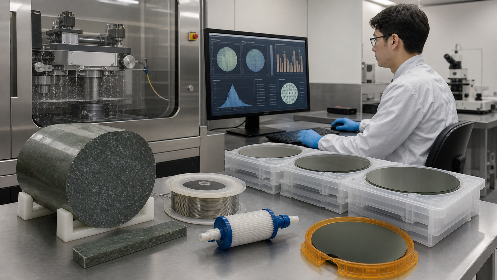
ewirexon diamond wire cutting systems for package material processing are characterized by an optimum price/performance ratio and are particularly suitable for precision cutting of chip carriers, lead frames and multi-layer packaging substrates. The systems generate ultra-high cutting accuracy with minimal kerf loss in limited production space. With rigid machine frames that can meet the strict precision requirements of advanced packaging, ewirexon offers an efficient and reliable option for fabs that handle both R&D prototyping and high-volume production at the same time. Thanks to a wide range of performance and customized process parameters, manufacturers of semiconductor packaging can reduce their component diversity with ewirexon’s Package Material Cutting solution.

  • Reduction of certification costs possible, as only a few reference system models need to be tested thanks to the scalability of the cutting system series.
  • Avoidance of re-certification effort by securing the certification basis with regard to manufacturing processes and materials.
  • Material and life cycle cost savings in high-volume operation through high yield compliance thanks to ultra-low kerf loss as well as component strength guaranteed by cycle testing.
  • Low installation and maintenance requirements, flexible placement options thanks to space-optimized machine design that minimizes stress on production lines and factory structure.
  • Compliance with semiconductor industry precision standards for certification possible, as diamond wire cutting systems can also be used for ultra-thin, multi-layer packaging materials.
  • Резка стружкодержателей и упаковочных материалов
  • Lead Frame & Substrate Slicing
  • Advanced Packaging & Microfabrication
  • Multi-Layer Brittle Material Processing
  • R&D Labs & High-Volume Fabs
НЕТ.ПараметрТехнические характеристики
1МодельTCQF400LNC-FM-HL
2Принцип резкиБесконечная алмазная леска / Механическая резка
3Функции резкиНарезка / Резка под углом и по профилю
4Максимальный размер заготовки (мм)Φ600 мм, высота 500 мм
5Размер рабочего стола (мм)Ø380 转台
6Точность плоскостности реза (мм)0.08
7Шероховатость поверхности (мкм)Ra 0,8 мкм
8Характеристики проволоки (мм)Ø0,65–1,0/2580
9Система натяженияКонтроль постоянного натяжения проволоки
10Количество направляющих колес4 колеса
11Приводной двигательСервомотор
12Скорость движения проволоки (м/с)51Max (регулируемый)
13Общая мощность (кВт)2.8
14Напряжение220 В, 50 Гц
15Система управленияСпециально разработанная система Tongcheng T32
16Габаритные размеры (Д × Ш × В) (мм)1350×1066×1968
17Брутто-вес, кг720
1

Maximum cutting precision, stable and high-yield

In the demanding semiconductor packaging industry, certified high-precision cutting solutions are indispensable. This case study looks at the complex challenge of developing a high-yield diamond wire cutting system that has to process ultra-thin, multi-layer packaging materials reliably with minimal kerf loss. How was our customer able to not only meet the strict precision requirements of advanced packaging, but even exceed them? What role did the strategic partnership with ewirexon play in this challenging project?

Хотите узнать больше о наших проектах? Не стесняйтесь, пишите нам!

Напишите нам!

Загрузите свои 2D-чертежи и как минимум один 3D-файл CAD, чтобы получить расчет стоимости быстрее и точнее. Если у вас несколько файлов, скомпрессируйте их в архив формата .zip или .rar. Предпочитаете электронную почту? Отправьте запрос на расчет стоимости по адресу info@xxx.com.

Новости и обновления