







PCB 기판 소재 절단


High-Precision Wire Saw Systems for Electronic Substrate Processing

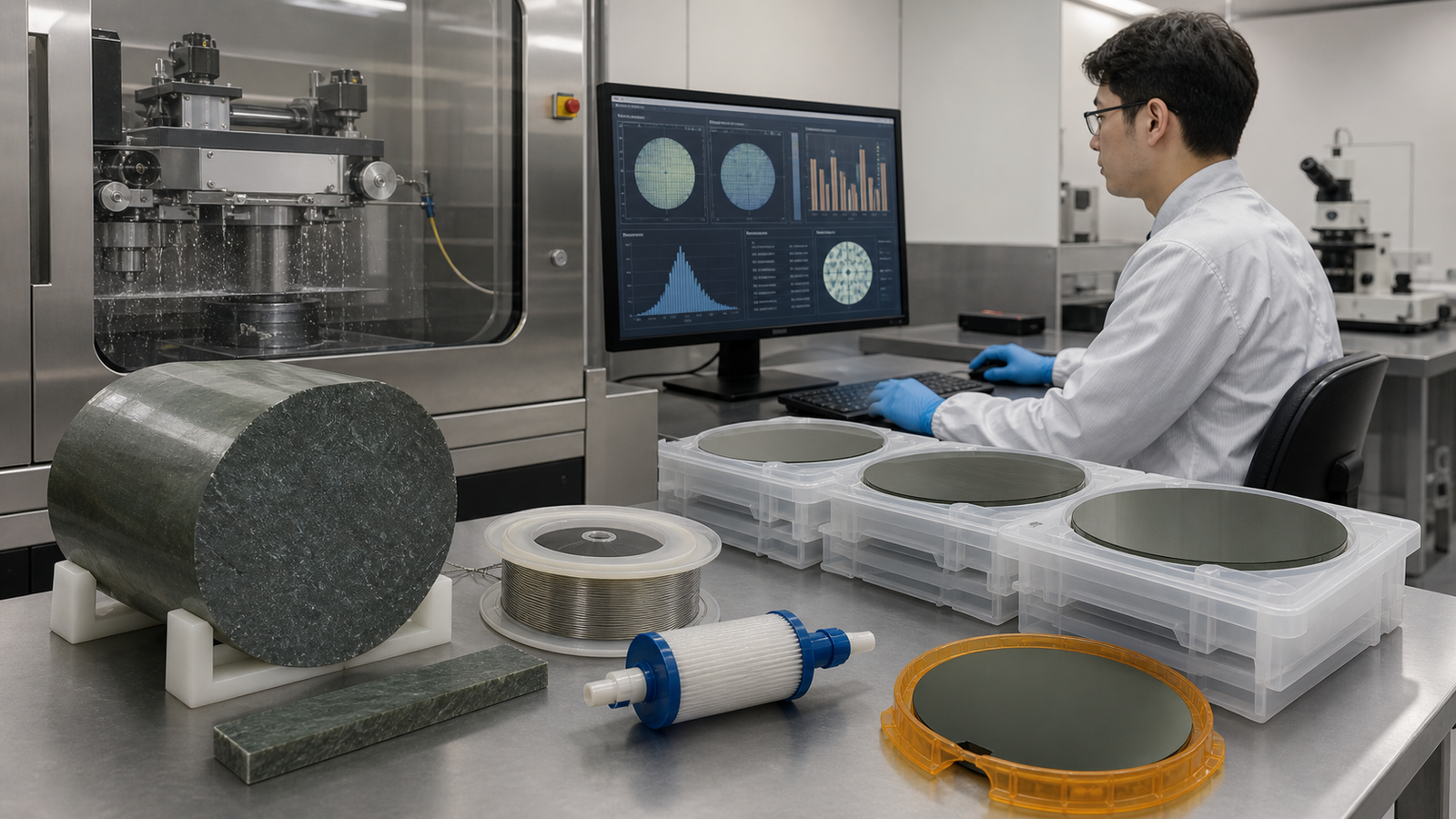
Rigid, flexible, and rigid-flex circuit substrates form the backbone of electronic devices, from consumer gadgets to industrial control systems. Precision slicing of these substrates is essential to maintain circuit integrity, flatness, and electrical performance. Diamond wire cutting provides a damage-free alternative to traditional methods, preserving substrate properties and eliminating delamination.

Our specialized systems deliver precise, clean slicing for FR-4, ceramic, polyimide, and copper-clad laminates, ensuring consistent thickness and flatness across large-format panels. The closed-loop tension control and real-time monitoring prevent micro-cracks and fiber damage, critical for high-density, fine-pitch circuit boards.

Suitable for both R&D prototyping and mass production, our solutions support high-throughput processing for multi-layer PCBs and advanced circuit substrates. The intelligent CNC control allows for precise parameter adjustment, ensuring compatibility with the latest PCB technologies and flexible circuit manufacturing processes.

Precision Slicing Systems for PCB & Circuit Substrates


Our diamond wire cutting solutions are tailored for high-precision slicing of rigid, flexible, and rigid-flex PCB base materials, ceramic substrates, and semiconductor packaging substrates. The systems feature closed-loop tension control and real-time monitoring, ensuring consistent thickness, flatness, and damage-free cutting for high-density, fine-pitch circuit boards. This eliminates delamination and micro-cracks, directly improving PCB yield and reliability in mass production.

회로 기판 및 PCB 베이스 재료 슬라이싱

장점
  • Damage-Free Processing: Prevents substrate delamination and fiber damage, critical for high-frequency PCB performance.
  • Consistent Thickness Control: Maintains uniform substrate thickness across large panels, ensuring stable circuit etching.
  • High Compatibility: Supports a full range of substrate materials, including FR-4, ceramic, polyimide, and copper-clad laminates.
  • High-Efficiency Mass Production: Multi-wire cutting design reduces processing time per panel, lowering production costs.
  • PCB base material slicing for consumer and automotive electronics
  • Ceramic substrate cutting for semiconductor packaging and power modules
  • Flexible circuit substrate processing for wearable and 5G devices
아니요.매개변수사양
1모델TCQF400LNC-FM-HL
2절단 원리무한 다이아몬드 와이어 / 물리적 절단
3절단 기능슬라이싱 / 각도 및 단면 절단
4최대 공작물 크기(mm)Φ600mm, 높이 500mm
5작업대 크기(mm)Ø380 转台
6절단 평탄도 정밀도(mm)0.08
7표면 거칠기(μm)Ra 0.8μm
8와이어 사양(mm)Ø0.65–1.0/2580
9장력 시스템일정한 와이어 장력 제어
10가이드 휠 수량4륜
11구동 모터서보 모터
12와이어 속도 (m/s)51Max(조절 가능)
13총 출력(kW)2.8
14전압220V 50Hz
15제어 시스템맞춤 개발된 통청 T32 시스템
16치수 (길이×폭×높이)(mm)1350×1066×1968
17총 중량 (kg)720
0

Read the Case: Improve PCB Base Material Slicing Quality

Professional PCB base material slicing enterprises adopted our solutions to upgrade equipment and workflows, gaining higher yield, lower waste and reliable slicing precision.
당사의 기술 사례에 대해 더 자세히 알고 싶으신가요? 언제든지 문의해 주세요.

문의해 주세요!

더 빠르고 정확한 견적을 받으시려면 2D 도면과 3D CAD 파일 1개 이상을 업로드해 주세요. 파일이 여러 개인 경우, .zip 또는 .rar 파일로 압축해 주시기 바랍니다. 이메일을 선호하시나요? 견적 요청(RFQ)을 info@xxx.com으로 보내주세요.

뉴스 및 업데이트