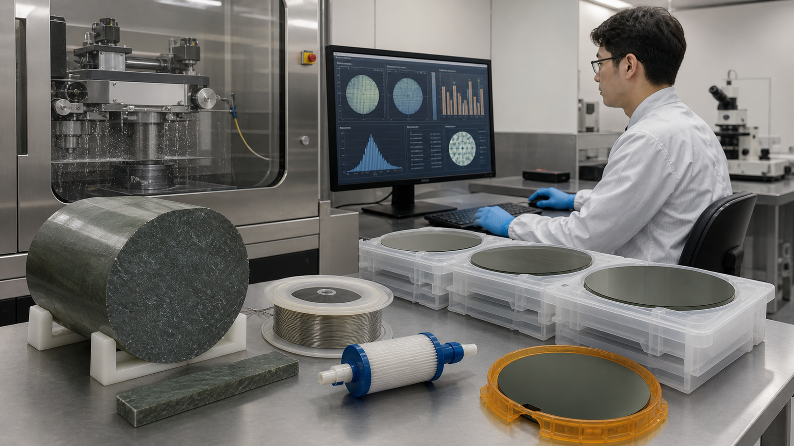









उच्च सटीकता वाली आधार सामग्री की कटाई


Ultra-Accurate Diamond Wire Systems for Advanced Substrates

High-value base materials such as optical glass, quartz, sapphire, and semiconductor substrates are essential components in precision optical, RF, and optoelectronic devices. Ultra-precise cutting is required to achieve tight tolerances, superior surface quality, and minimal material loss in these high-value applications.

Our high-precision cutting systems deliver industry-leading accuracy, ensuring clean, burr-free cuts with exceptional dimensional consistency. The advanced cooling and tension control systems protect delicate substrates, maintaining their optical, electrical, and mechanical properties for critical applications.

Designed to support both R&D prototyping and large-scale manufacturing, our systems offer scalable performance and versatile material compatibility. The intelligent control interface allows for easy parameter adjustment, ensuring optimal performance across a wide range of advanced base materials and processing requirements.

Ultra-Precision Diamond Wire Cutting for Base Materials

Our high-precision base material cutting systems deliver industry-leading accuracy for a full range of advanced base materials, including optical glass, quartz, sapphire, and semiconductor substrates. Designed for R&D prototyping and high-volume mass production, these systems achieve tight-tolerance slicing with superior surface quality, eliminating the need for extensive post-processing. The intelligent cutting algorithms and constant temperature control ensure consistent performance across diverse material types and thicknesses.

उच्च-सटीकता आधार सामग्री काटने

लाभ
  • Industry-Leading Precision: Tight tolerance control meets the strict requirements of optical and semiconductor manufacturing.
  • Superior Surface Quality: Low-damage cutting reduces polishing time and costs, improving production efficiency.
  • Versatile Material Support: Processes optical glass, quartz, sapphire, silicon, and other high-value base materials.
  • Scalable Production: Flexible configurations for lab R&D, pilot lines, and full-scale mass production.
  • Optical glass and quartz substrate cutting for optical devices and semiconductors
  • Sapphire wafer slicing for LED and RF devices
  • High-precision base material processing for aerospace and medical electronics
नहीं।.पैरामीटरविनिर्देश
1मॉडलटीसीक्यूएफ400एलएनसी-एफएम-एचएल
2काटन का सिद्धांतअनंत हीरे की तार / भौतिक काटना
3काटने के कार्यस्लाइसिंग / कोण और प्रोफ़ाइल कटिंग
4अधिकतम वर्कपीस आकार (मिमी)Φ600 मिमी, ऊँचाई 500 मिमी
5कार्य-टेबल का आकार (मिमी)Ø380 转台
6कटिंग समतलता सटीकता (मिमी)0.08
7सतही खुरदरापन (माइक्रोमीटर)रे 0.8 माइक्रोमीटर
8तार विनिर्देश (मिमी)Ø0.65–1.0/2580
9तनाव प्रणालीसतत तार तनाव नियंत्रण
10गाइड व्हील की मात्राचार पहिये
11चालक मोटरसर्भो मोटर
12तार की गति (मी/से)51मैक्स (समायोज्य)
13कुल शक्ति (किलोवाट)2.8
14वोल्टेज220v 50Hz
15नियंत्रण प्रणालीविशेष रूप से विकसित टोंगचेंग टी32 प्रणाली
16फुटप्रिंट (लंबाई×चौड़ाई×ऊंचाई)(मिमी)१३५०×१०६६×१९६८
17कुल वजन किग्रा720
8

Case Learning: Achieve Top-tier Precision in Base Material Cutting

Process upgrades for high-precision base material cutting greatly improved yield, enhanced material utilization and maintained long-term precision stability.
हमारे तकनीकी मामलों के बारे में और जानें? कृपया संपर्क करें।.

हमें लिखें!

तेज़ और अधिक सटीक कोटेशन के लिए अपनी 2D ड्रॉइंग्स और कम से कम एक 3D CAD फ़ाइल अपलोड करें। यदि आपके पास कई फ़ाइलें हैं, तो कृपया उन्हें .zip या .rar में संपीड़ित करें। ईमेल पसंद है? अपना RFQ info@xxx.com पर भेजें।.

समाचार और अपडेट